SLPS405F March 2013 – March 2015 CSD87381P
PRODUCTION DATA.
- 1Features
- 2Applications
- 3Description
- 4Revision History
- 5Specifications
- 6Application and Implementation
- 7Layout
- 8Device and Documentation Support
- 9Mechanical, Packaging, and Orderable Information
Package Options
Mechanical Data (Package|Pins)
- MPC|5
Thermal pad, mechanical data (Package|Pins)
Orderable Information
9 Mechanical, Packaging, and Orderable Information
The following pages include mechanical, packaging, and orderable information. This information is the most current data available for the designated devices. This data is subject to change without notice and revision of this document. For browser-based versions of this data sheet, refer to the left-hand navigation.
9.1 CSD87381P Package Dimensions

Pin Configuration
| Position | Designation |
|---|---|
| Pin 1 | TG |
| Pin 2 | VIN |
| Pin 3 | PGND |
| Pin 4 | BG |
| Pin 5 | VSW |
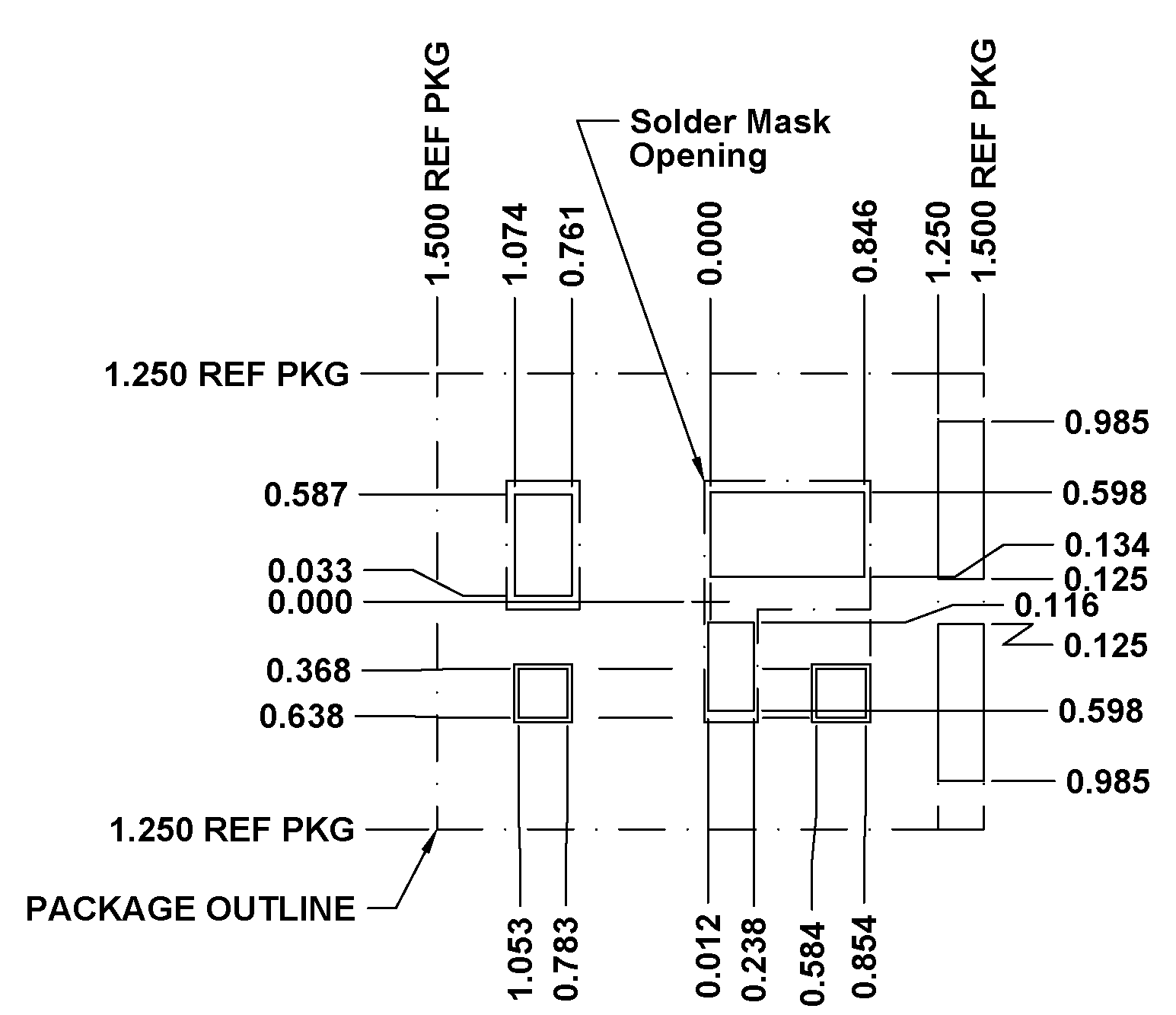
9.2 Land Pattern Recommendation

9.3 Stencil Recommendation (100 µm)

9.4 Stencil Recommendation (125 µm)

For recommended circuit layout for PCB designs, see application note SLPA005 – Reducing Ringing Through PCB Layout Techniques.
9.5 Pin Drawing

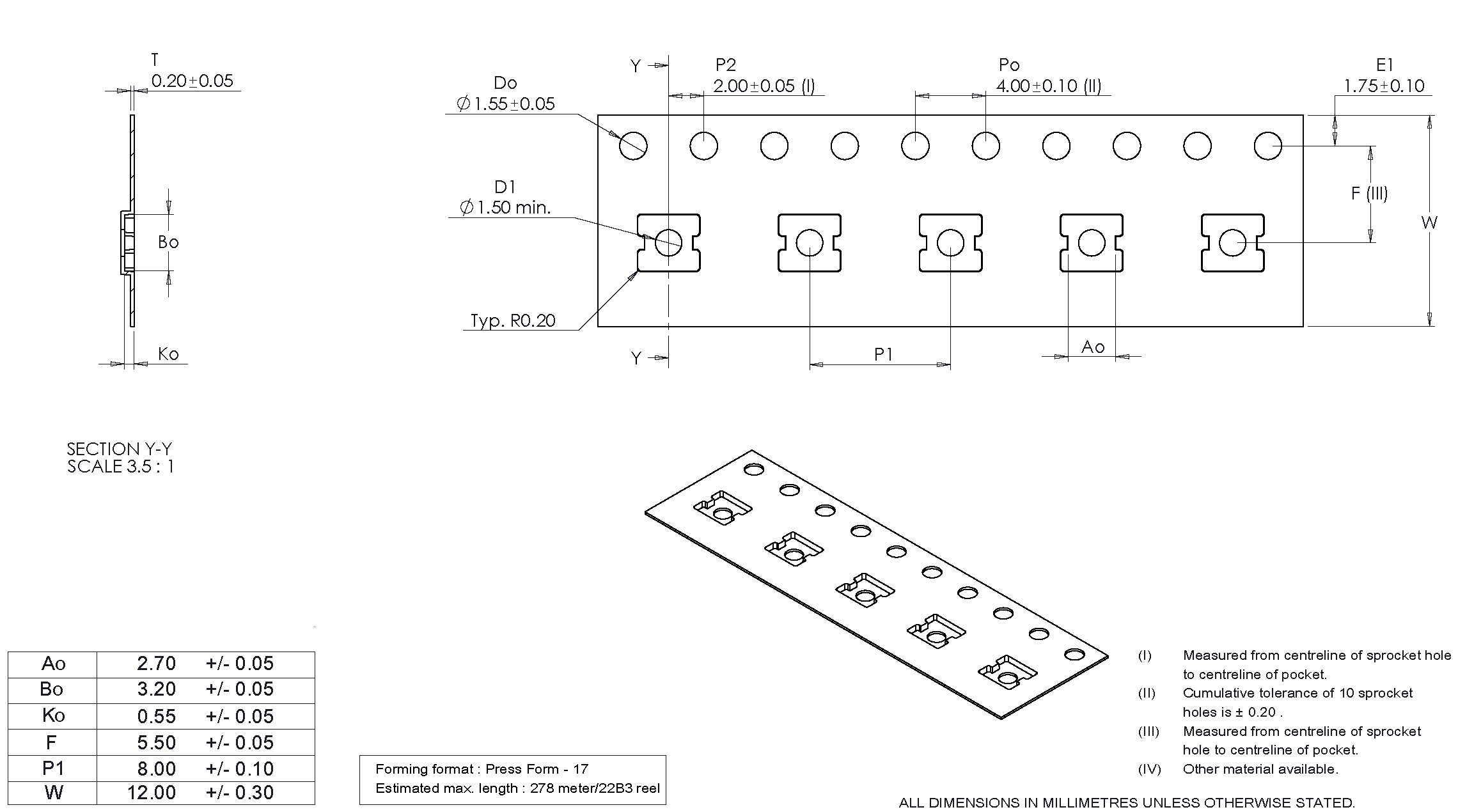
9.6 CSD87381P Embossed Carrier Tape Dimensions

1. Pin 1 is oriented in the top-left quadrant of the tape enclosure (closest to the carrier tape sprocket holes).