-
CSD87384M Synchronous Buck NexFET Power Block II
Package Options
Mechanical Data (Package|Pins)
- MPB|5
Thermal pad, mechanical data (Package|Pins)
Orderable Information
CSD87384M Synchronous Buck NexFET Power Block II
1 Features
- Half-Bridge Power Block
- 90.5% System Efficiency at 25 A
- Up to 30 A Operation
- High Density – 5 mm x 3.5 mm LGA Footprint
- Double-Side Cooling Capability
- Ultra-Low Profile – 0.48 mm Max
- Optimized for 5 V Gate Drive
- Low Switching Losses
- Ultra-Low Inductance Package
- RoHS Compliant
- Halogen Free
- Pb-Free
2 Applications
- Synchronous Buck Converters
- High Frequency Applications
- High Current, Low Duty Cycle Applications
- Multiphase Synchronous Buck Converters
- POL DC-DC Converters
3 Description
The CSD87384M NexFET™ Power Block II is a highly optimized design for synchronous buck applications offering high current and high efficiency capability in a small 5.0 mm × 3.5 mm outline. Optimized for 5 V gate drive applications, this product offers an efficient and flexible solution capable of providing a high density power supply when paired with any 5 V gate drive from an external controller or driver.
Ordering Information(1)
| Device | Media | Qty | Package | Ship |
|---|---|---|---|---|
| CSD87384M | 13-Inch Reel | 2500 | 5 × 3.5 LGA | Tape and Reel |
| CSD87384MT | 7-Inch Reel | 250 |
- For all available packages, see the orderable addendum at the end of the data sheet.
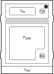
Typical Circuit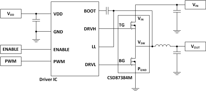 |
Typical Power Block Efficiency and Power Loss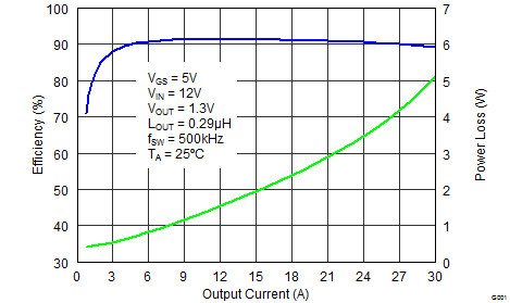 |
4 Revision History
Changes from C Revision (May 2014) to D Revision
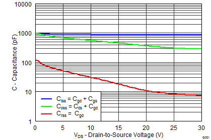
- Changed capacitance units to read pF in Figure 15Go
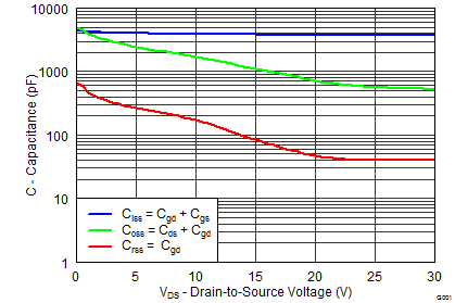
- Changed capacitance units to read pF in Figure 16Go
Changes from A Revision (September 2013) to B Revision
Changes from * Revision (September 2013) to A Revision
- Changed VGS(th) from 1.0 V to 1.1 V in the Electrical Characteristics tableGo
5 Specifications
5.1 Absolute Maximum Ratings
TA = 25°C (unless otherwise noted) (1)| MIN | MAX | UNIT | |||
|---|---|---|---|---|---|
| Voltage | VIN to PGND | –0.8 | 30 | V | |
| VSW to PGND | 30 | ||||
| VSW to PGND (10 ns) | 32 | ||||
| TG to VSW | –8 | 10 | |||
| BG to PGND | –8 | 10 | |||
| IDM | Pulsed Current Rating(2) | 95 | A | ||
| PD | Power Dissipation(3) | 8 | W | ||
| EAS | Avalanche Energy | Sync FET, ID = 68, L = 0.1 mH | 231 | mJ | |
| Control FET, ID = 31, L = 0.1 mH | 48 | ||||
| TJ | Operating Junction | –55 | 150 | °C | |
| Tstg | Storage Temperature Range | –55 | 150 | °C | |
5.2 Recommended Operating Conditions
TA = 25°C (unless otherwise noted)| MIN | MAX | UNIT | |||
|---|---|---|---|---|---|
| VGS | Gate Drive Voltage | 4.5 | 8 | V | |
| VIN | Input Supply Voltage | 24 | V | ||
| ƒSW | Switching Frequency | CBST = 0.1 μF (min) | 200 | 1500 | kHz |
| Operating Current | No Airflow | 30 | A | ||
| With Airflow (200 LFM) | 35 | A | |||
| With Airflow + Heat Sink | 40 | A | |||
| TJ | Operating Temperature | 125 | °C | ||
5.3 Power Block Performance
TA = 25°C (unless otherwise noted)| PARAMETER | CONDITIONS | MIN | TYP | MAX | UNIT | |
|---|---|---|---|---|---|---|
| PLOSS | Power Loss(1) | VIN = 12 V, VGS = 5 V VOUT = 1.3 V, IOUT = 25 A fSW = 500 kHz LOUT = 0.3 µH, TJ = 25ºC |
3.7 | W | ||
| IQVIN | VIN Quiescent Current | TG to TGR = 0 V BG to PGND = 0 V |
10 | µA | ||
5.4 Thermal Information
TA = 25°C (unless otherwise stated)| THERMAL METRIC | MIN | TYP | MAX | UNIT | |
|---|---|---|---|---|---|
| RθJA | Junction-to-ambient thermal resistance (Min Cu) (2) | 153 | °C/W | ||
| Junction-to-ambient thermal resistance (Max Cu) (1)(2) | 67 | ||||
| RθJC | Junction-to-case thermal resistance (Top of package) (2) | 3.0 | |||
| Junction-to-case thermal resistance (PGND Pin) (2) | 1.25 | ||||
(3.81 cm × 3.81 cm), 0.06 inch (1.52 mm) thick FR4 board. RθJC is specified by design while RθJA is determined by the user’s board design.
5.5 Electrical Characteristics
TA = 25°C (unless otherwise stated)| PARAMETER | TEST CONDITIONS | Q1 Control FET | Q2 Sync FET | UNIT | ||||||
|---|---|---|---|---|---|---|---|---|---|---|
| MIN | TYP | MAX | MIN | TYP | MAX | |||||
| STATIC CHARACTERISTICS | ||||||||||
| BVDSS | Drain-to-Source Voltage | VGS = 0 V, IDS = 250 μA | 30 | 30 | V | |||||
| IDSS | Drain-to-Source Leakage Current | VGS = 0 V, VDS = 24 V | 1 | 1 | μA | |||||
| IGSS | Gate-to-Source Leakage Current | VDS = 0 V, VGS = 10 V | 100 | 100 | nA | |||||
| VGS(th) | Gate-to-Source Threshold Voltage | VDS = VGS, IDS = 250 μA | 1.1 | 1.9 | 1.1 | 1.7 | V | |||
| RDS(on) | Drain-to-Source On-Impedance | VGS = 4.5 V, IDS = 25 A | 7.5 | 8.9 | 2.15 | 2.6 | mΩ | |||
| VGS = 8 V, IDS = 25 A | 6.4 | 7.7 | 1.95 | 2.4 | ||||||
| gƒs | Transconductance | VDS = 10 V, IDS = 25 A | 67 | 240 | S | |||||
| DYNAMIC CHARACTERISTICS | ||||||||||
| CISS | Input Capacitance (1) | VGS = 0 V, VDS = 15 V, f = 1MHz |
884 | 1150 | 3760 | 4890 | pF | |||
| COSS | Output Capacitance (1) | 452 | 588 | 1110 | 1440 | pF | ||||
| CRSS | Reverse Transfer Capacitance (1) | 19.4 | 25.2 | 87 | 114 | pF | ||||
| RG | Series Gate Resistance (1) | 1.0 | 2.0 | 0.7 | 1.4 | Ω | ||||
| Qg | Gate Charge Total (4.5 V) (1) | VDS = 15 V, IDS = 25 A |
7.1 | 9.2 | 31 | 40 | nC | |||
| Qgd | Gate Charge – Gate-to-Drain | 1.5 | 8.6 | nC | ||||||
| Qgs | Gate Charge – Gate-to-Source | 2.7 | 8.6 | nC | ||||||
| Qg(th) | Gate Charge at Vth | 1.3 | 5.4 | nC | ||||||
| QOSS | Output Charge | VDD = 12 V, VGS = 0 V | 11.3 | 37 | nC | |||||
| td(on) | Turn On Delay Time | VDS = 15 V, VGS = 4.5 V, IDS = 25 A, RG = 2 Ω |
8.7 | 17.5 | ns | |||||
| tr | Rise Time | 56 | 49 | ns | ||||||
| td(off) | Turn-Off Delay Time | 14 | 29 | ns | ||||||
| tƒ | Fall Time | 7.6 | 8.2 | ns | ||||||
| DIODE CHARACTERISTICS | ||||||||||
| VSD | Diode Forward Voltage | IDS = 25 A, VGS = 0 V | 0.85 | 0.80 | V | |||||
| Qrr | Reverse Recovery Charge | Vdd = 15 V, IF = 25 A, di/dt = 300 A/μs |
21 | 51 | nC | |||||
| trr | Reverse Recovery Time | 21 | 32 | ns | ||||||
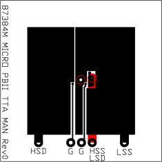 |
Max RθJA = 67°C/W when mounted on 1 inch2 (6.45 cm2) of 2 oz. (0.071 mm thick) Cu. |
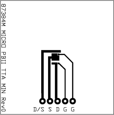 |
Max RθJA = 153°C/W when mounted on minimum pad area of 2 oz. (0.071 mm thick) Cu. |
5.6 Typical Power Block Device Characteristics
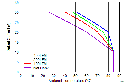
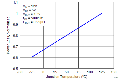
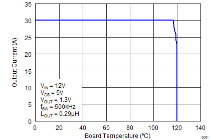
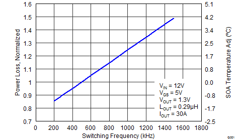
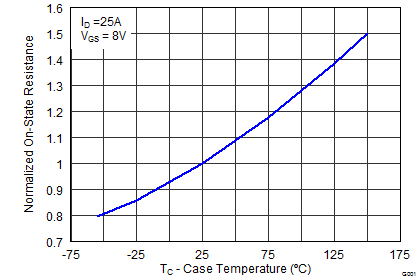
TJ = 125°C, unless stated otherwise. For Figure 3 and Figure 4, the Typical Power Block System Characteristic curves are based on measurements made on a PCB design with dimensions of 4.0 inches (W) × 3.5 inches (L) × 0.062 inch (H) and 6 copper layers of 1 oz. copper thickness. See Application and Implementation for detailed explanation.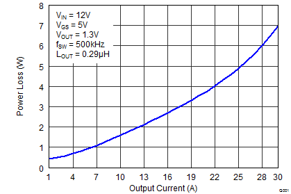
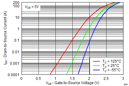
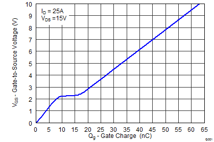
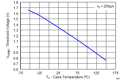
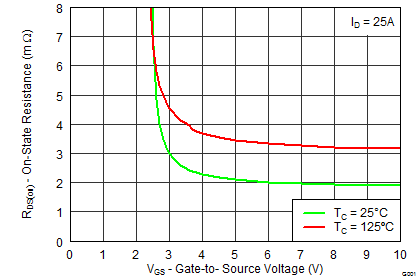
5.7 Typical Power Block MOSFET Characteristics
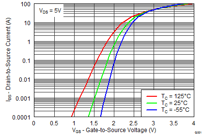
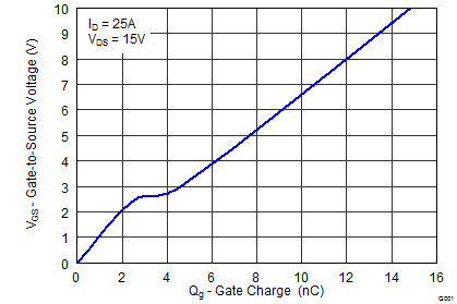
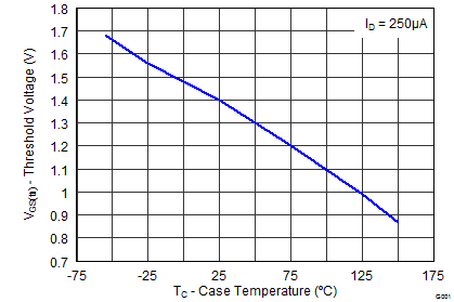
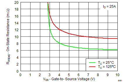
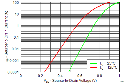
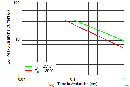
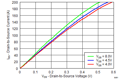
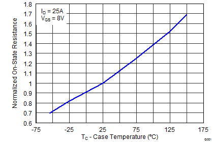
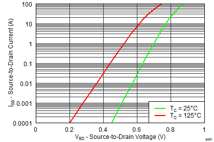
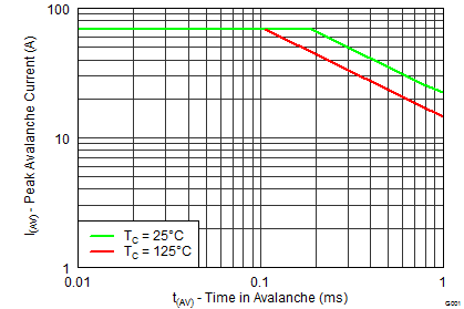
TA = 25°C, unless stated otherwise.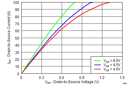
6 Application and Implementation
NOTE
Information in the following applications sections is not part of the TI component specification, and TI does not warrant its accuracy or completeness. TI ’ s customers are responsible for determining suitability of components for their purposes. Customers should validate and test their design implementation to confirm system functionality.
6.1 Application Information
The CSD87384M NexFET™ power block is an optimized design for synchronous buck applications using 5 V gate drive. The Control FET and Sync FET silicon are parametrically tuned to yield the lowest power loss and highest system efficiency. As a result, a new rating method is needed which is tailored toward a more systems-centric environment. System level performance curves such as Power Loss, Safe Operating Area, and normalized graphs allow engineers to predict the product performance in the actual application.
6.2 Power Loss Curves
MOSFET-centric parameters such as RDS(ON) and Qgd are needed to estimate the loss generated by the devices. To simplify the design process for engineers, TI has provided measured power loss performance curves. Figure 1 plots the power loss of the CSD87384M as a function of load current. This curve is measured by configuring and running the CSD87384M as it would be in the final application (see Figure 27). The measured power loss is the CSD87384M loss and consists of both input conversion loss and gate drive loss. Equation 1 is used to generate the power loss curve.
The power loss curve in Figure 1 is measured at the maximum recommended junction temperatures of 125°C under isothermal test conditions.
6.3 Safe Operating Curves (SOA)
The SOA curves in the CSD87384M data sheet provide guidance on the temperature boundaries within an operating system by incorporating the thermal resistance and system power loss. Figure 3 to Figure 4 outline the temperature and airflow conditions required for a given load current. The area under the curve dictates the safe operating area. All the curves are based on measurements made on a PCB design with dimensions of 4 inches (W) × 3.5 inches (L) × 0.062 inch (T) and 6 copper layers of 1 oz. copper thickness.
6.4 Normalized Curves
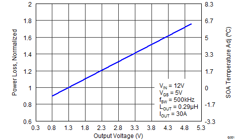
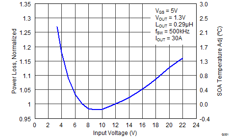
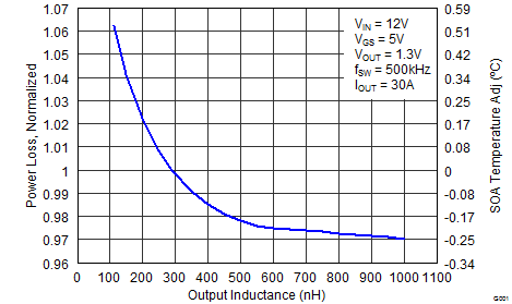
The normalized curves in the CSD87384M data sheet provide guidance on the Power Loss and SOA adjustments based on their application-specific needs. These curves show how the power loss and SOA boundaries adjust for a given set of systems conditions. The primary y-axis is the normalized change in power loss and the secondary y-axis is the change in system temperature required to comply with the SOA curve. The change in power loss is a multiplier for the Power Loss curve and the change in temperature is subtracted from the SOA curve.
 Figure 27. Typical Application
6.5 Calculating Power Loss and SOA
The user can estimate product loss and SOA boundaries by arithmetic means (see Design Example). Though the Power Loss and SOA curves in this data sheet are taken for a specific set of test conditions, the following procedure outlines the steps the user should take to predict product performance for any set of system conditions.
6.5.1 Design Example
Operating Conditions:
- Output Current = 20 A
- Input Voltage = 4 V
- Output Voltage = 1 V
- Switching Frequency = 800 kHz
- Inductor = 0.2 µH
6.5.2 Calculating Power Loss
- Power Loss at 20 A = 3.5 W (Figure 1)
- Normalized Power Loss for input voltage ≈ 1.18 (Figure 6)
- Normalized Power Loss for output voltage ≈ 0.94 (Figure 7)
- Normalized Power Loss for switching frequency ≈ 1.15 (Figure 5)
- Normalized Power Loss for output inductor ≈ 1.02 (Figure 8)
- Final calculated Power Loss = 3.5 W × 1.18 × 0.94 × 1.15 × 1.02 ≈ 4.6 W
6.5.3 Calculating SOA Adjustments
In the previous design example, the estimated power loss of the CSD87384M would increase to 4.6 W. In addition, the maximum allowable board and/or ambient temperature would have to decrease by 2.4ºC. Figure 28 graphically shows how the SOA curve would be adjusted accordingly.
- Start by drawing a horizontal line from the application current to the SOA curve.
- Draw a vertical line from the SOA curve intercept down to the board or ambient temperature.
- Adjust the SOA board/ambient temperature by subtracting the temperature adjustment value.
In the design example, the SOA temperature adjustment yields a reduction in allowable board/ambient temperature of 2.4ºC. In the event the adjustment value is a negative number, subtracting the negative number would yield an increase in allowable board or ambient temperature.
 Figure 28. Power Block SOA
