SLPS598E May 2017 – June 2024 CSD88584Q5DC
PRODUCTION DATA
- 1
- 1Features
- 2Applications
- 3Description
- 4Specifications
-
5Application and Implementation
- 5.1 Application Information
- 5.2 Brushless DC Motor With Trapezoidal Control
- 5.3 Power Loss Curves
- 5.4 Safe Operating Area (SOA) Curve
- 5.5 Normalized Power Loss Curves
- 5.6 Design Example – Regulate Current to Maintain Safe Operation
- 5.7 Design Example – Regulate Board and Case Temperature to Maintain Safe Operation
- 6Layout
- 7Device and Documentation Support
- 8Revision History
- 9Mechanical, Packaging, and Orderable Information
Package Options
Mechanical Data (Package|Pins)
- DMM|22
Thermal pad, mechanical data (Package|Pins)
Orderable Information
6.2 Layout Example
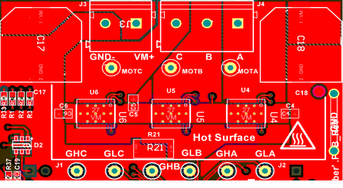
 Figure 6-2 Top
Layer
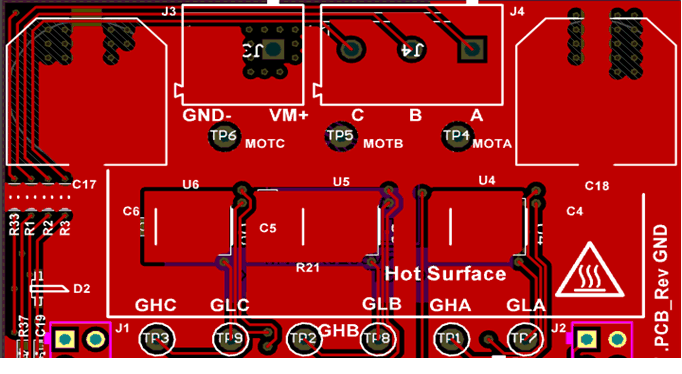
 Figure 6-3 Bottom
Layer
Figure 6-3 Bottom
LayerThe placement of the input capacitors C4, C5, and C6 relative to VIN and PGND pins of CSD88584Q5DC device should have the highest priority during the component placement routine. It is critical to minimize the VIN to GND parasitic loop inductance. A shunt resistor R21 is used between all three U4, U5, and U6 power block source terminals to the input supply GND return pin.
Input RMS current filtering is achieved via two bulk caps C17 and C18. Based on the RMS current ratings, the recommended part number for input bulk is CAP AL, 330µF, 63V, ±20%, PN: EMVA630ADA331MKG5S.