SLPS597D April 2017 – June 2024 CSD88599Q5DC
PRODUCTION DATA
- 1
- 1Features
- 2Applications
- 3Description
- 4Specifications
-
5Application and Implementation
- 5.1 Application Information
- 5.2 Brushless DC Motor With Trapezoidal Control
- 5.3 Power Loss Curves
- 5.4 Safe Operating Area (SOA) Curve
- 5.5 Normalized Power Loss Curves
- 5.6 Design Example – Regulate Current to Maintain Safe Operation
- 5.7 Design Example – Regulate Board and Case Temperature to Maintain Safe Operation
- 5.8 Layout
- 6Device and Documentation Support
- 7Revision History
- 8Mechanical, Packaging, and Orderable Information
Package Options
Refer to the PDF data sheet for device specific package drawings
Mechanical Data (Package|Pins)
- DMM|22
Thermal pad, mechanical data (Package|Pins)
Orderable Information
2 Applications
- Three-phase bridge for brushless DC motor control
- Up to 12s battery power tools
- Other half and full bridge topologies
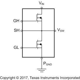
 Power Block
Schematic