SLPS597D April 2017 – June 2024 CSD88599Q5DC
PRODUCTION DATA
- 1
- 1Features
- 2Applications
- 3Description
- 4Specifications
-
5Application and Implementation
- 5.1 Application Information
- 5.2 Brushless DC Motor With Trapezoidal Control
- 5.3 Power Loss Curves
- 5.4 Safe Operating Area (SOA) Curve
- 5.5 Normalized Power Loss Curves
- 5.6 Design Example – Regulate Current to Maintain Safe Operation
- 5.7 Design Example – Regulate Board and Case Temperature to Maintain Safe Operation
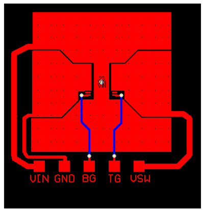
- 5.8 Layout
- 6Device and Documentation Support
- 7Revision History
- 8Mechanical, Packaging, and Orderable Information
Package Options
Mechanical Data (Package|Pins)
- DMM|22
Thermal pad, mechanical data (Package|Pins)
4.5 Electrical Characteristics
TJ = 25°C (unless otherwise stated)
| PARAMETER | TEST CONDITIONS | MIN | TYP | MAX | UNIT | ||
|---|---|---|---|---|---|---|---|
| STATIC CHARACTERISTICS | |||||||
| BVDSS | Drain-to-source voltage | VGS = 0V, IDS = 250µA | 60 | V | |||
| IDSS | Drain-to-source leakage current | VGS = 0V, VDS = 48V | 1 | µA | |||
| IGSS | Gate-to-source leakage current | VDS = 0V, VGS = 20V | 100 | nA | |||
| VGS(th) | Gate-to-source threshold voltage | VDS = VGS, IDS = 250µA | 1.4 | 2.0 | 2.5 | V | |
| RDS(on) | Drain-to-source on-resistance | VGS = 4.5V, IDS = 30A | 2.5 | 3.3 | mΩ | ||
| VGS = 10V, IDS = 30A | 1.7 | 2.1 | |||||
| gfs | Transconductance | VDS = 6V, IDS = 30A | 130 | S | |||
| DYNAMIC CHARACTERISTICS | |||||||
| CISS | Input capacitance | VGS =
0V, VDS = 30V, ƒ = 1MHz | 3720 | 4840 | pF | ||
| COSS | Output capacitance | 670 | 870 | pF | |||
| CRSS | Reverse transfer capacitance | 12 | 16 | pF | |||
| RG | Series gate resistance | 0.9 | 1.8 | Ω | |||
| Qg | Gate charge total (4.5 V) | VDS =
30V, IDS = 30A | 21 | 27 | nC | ||
| Qg | Gate charge total (10 V) | 43 | 56 | nC | |||
| Qgd | Gate charge gate-to-drain | 7.0 | nC | ||||
| Qgs | Gate charge gate-to-source | 10.1 | nC | ||||
| Qg(th) | Gate charge at Vth | 6.3 | nC | ||||
| QOSS | Output charge | VDS = 30V, VGS = 0V | 100 | nC | |||
| td(on) | Turnon delay time | VDS =
30V, VGS = 10V, IDS = 30A, RG = 0Ω | 9 | ns | |||
| tr | Rise time | 20 | ns | ||||
| td(off) | Turnoff delay time | 23 | ns | ||||
| tf | Fall time | 3 | ns | ||||
| DIODE CHARACTERISTICS | |||||||
| VSD | Diode forward voltage | IDS = 30A, VGS = 0V | 0.8 | 1.0 | V | ||
| Qrr | Reverse recovery charge | VDS =
30V, IF = 30A, di/dt = 300A/µs | 172 | nC | |||
| trr | Reverse recovery time | 36 | ns | ||||
| Max RθJA = 50°C/W when mounted on 1in2 (6.45cm2) of 2oz (0.071mm) thick Cu. | 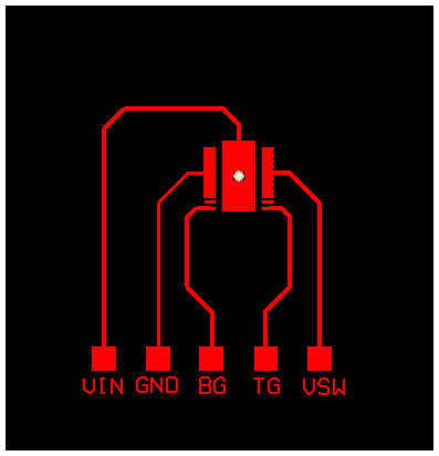
| Max RθJA = 125°C/W when mounted on minimum pad area of 2oz (0.071mm) thick Cu. |