SLPS597D April 2017 – June 2024 CSD88599Q5DC
PRODUCTION DATA
- 1
- 1Features
- 2Applications
- 3Description
- 4Specifications
-
5Application and Implementation
- 5.1 Application Information
- 5.2 Brushless DC Motor With Trapezoidal Control
- 5.3 Power Loss Curves
- 5.4 Safe Operating Area (SOA) Curve
- 5.5 Normalized Power Loss Curves
- 5.6 Design Example – Regulate Current to Maintain Safe Operation
- 5.7 Design Example – Regulate Board and Case Temperature to Maintain Safe Operation
- 5.8 Layout
- 6Device and Documentation Support
- 7Revision History
- 8Mechanical, Packaging, and Orderable Information
Package Options
Refer to the PDF data sheet for device specific package drawings
Mechanical Data (Package|Pins)
- DMM|22
Thermal pad, mechanical data (Package|Pins)
Orderable Information
5.6 Design Example – Regulate Current to Maintain Safe Operation
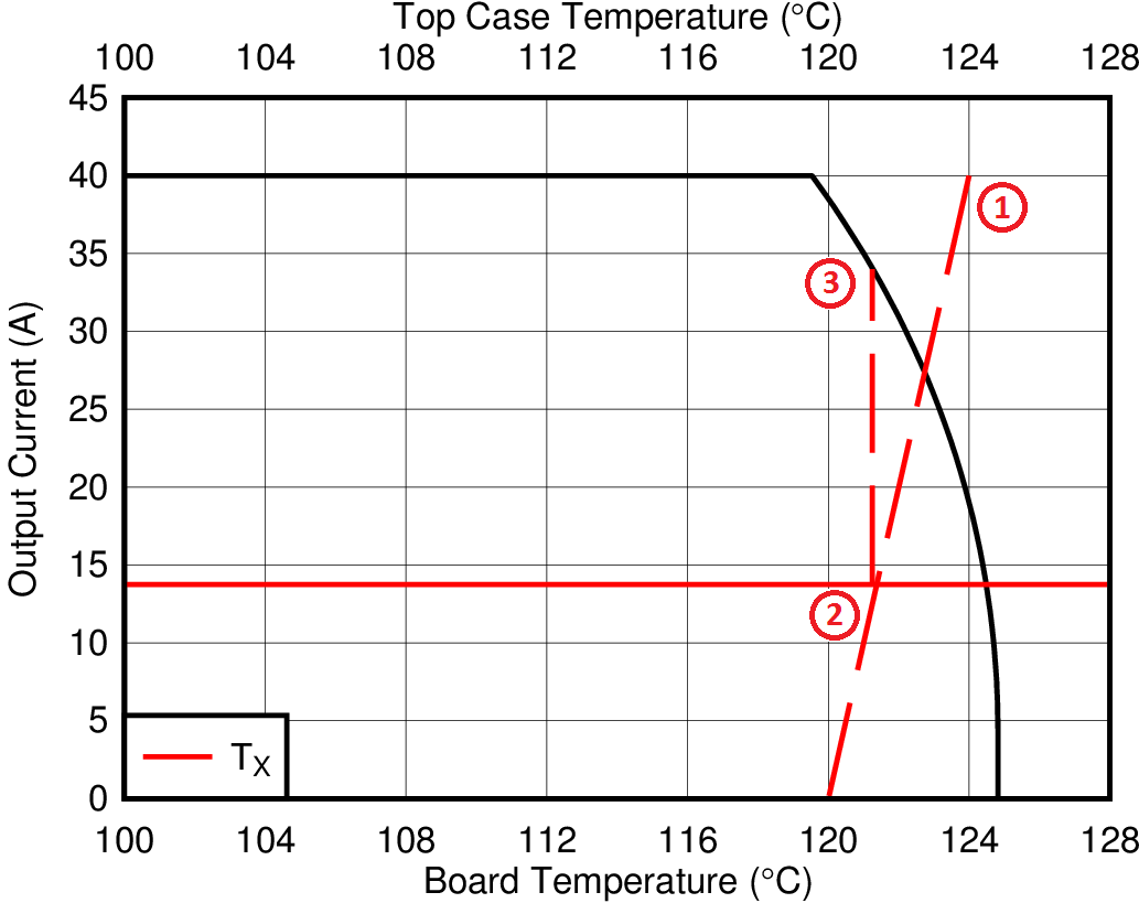
If the case and board temperature of the power block are known, the SOA can be used to determine the maximum allowed current that will maintain operation within the safe operating area of the device. The following procedure outlines how to determine the RMS current limit while maintaining operation within the confines of the SOA, assuming the temperatures of the top of the package and PCB directly underneath the part are known.
- Start at the maximum current of the device on the Y-axis and draw a line from this point at the known top case temperature to the known PCB temperature.
- Observe where this point intersects the TX line.
- At this intersection with the TX line, draw vertical line until you hit the SOA current limit. This intercept is the maximum allowed current at the corresponding power block PCB and case temperatures.
In the example below, we show how to achieve this for the temperatures TC = 124°C and TB = 120°C. First we draw from 40 A on the Y-axis at 124°C to 120°C on the X-axis. Then, we draw a line up from where this line crosses the TX line to see that this line intercepts the SOA at 34A. Thus we can assume if we are measuring a PCB temperature of 124°C, and a top case temperature of 120°C, the power block can handle 34A RMS, at the normalized conditions. At conditions that differ from those in Figure 4-1, the user may be required to make an SOA temperature adjustment on the TX line, as shown in the next section.
 Figure 5-4 Regulating Current to Maintain Safe Operation