SLPS723 September 2020 CSD95410RRB
PRODUCTION DATA
- 1Features
- 2Applications
- 3Description
- 4Revision History
- 5Device and Documentation Support
- 6Mechanical, Packaging, and Orderable Information
Package Options
Mechanical Data (Package|Pins)
- RRB|41
Thermal pad, mechanical data (Package|Pins)
Orderable Information
6.1 Mechanical Drawing
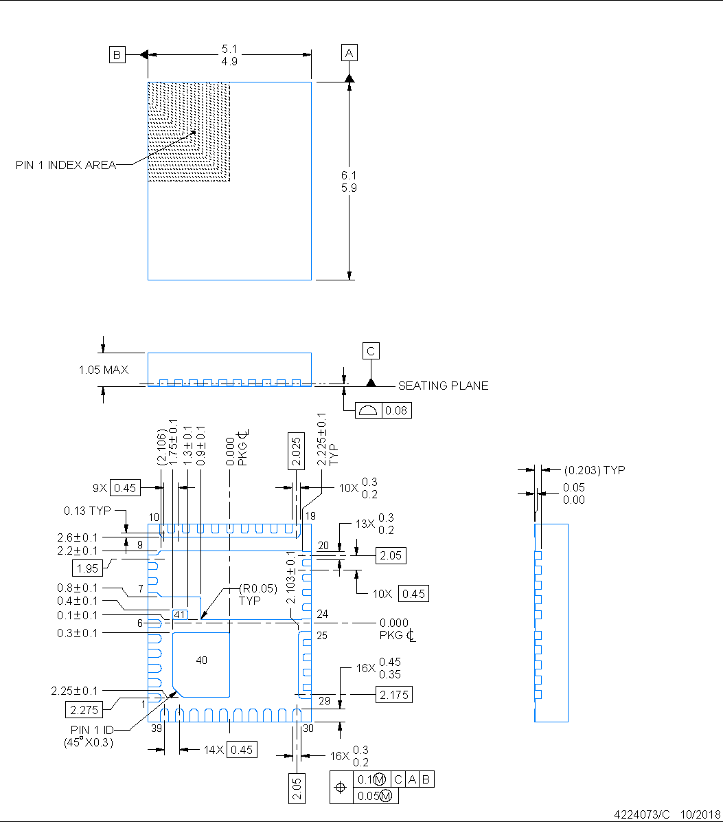
- All linear dimensions are in millimeters. Any dimensions in parenthesis are for reference only. Dimensioning and tolerancing per ASME Y14.5M.
- This drawing is subject to change without notice.
- The package thermal pads must be soldered to the printed circuit board for optimal thermal and mechanical performance.