SLPS671A June 2017 – January 2018 CSD95495QVM
PRODUCTION DATA.
- 1Features
- 2Applications
- 3Description
- 4Revision History
- 5Pin Configuration and Functions
- 6Specifications
- 7Application Schematic
- 8Device and Documentation Support
- 9Mechanical, Packaging, and Orderable Information
Package Options
Mechanical Data (Package|Pins)
- DMH|18
Thermal pad, mechanical data (Package|Pins)
Orderable Information
3 Description
The CSD95495QVM NexFET™ power stage is a highly optimized design for use in a high-power, high-density synchronous buck converter. This product integrates the driver IC and power MOSFETs to complete the power stage switching function. This combination produces high-current, high-efficiency, and high-speed switching capability in a small 4-mm × 5-mm outline package. It also integrates the accurate current sensing and temperature sensing functionality to simplify system design and improve accuracy. In addition, the PCB footprint has been optimized to help reduce design time and simplify the completion of the overall system design.
Device Information(1)
| DEVICE | MEDIA | QTY | PACKAGE | SHIP |
|---|---|---|---|---|
| CSD95495QVM | 13-Inch Reel | 2500 | VSON 4.00-mm × 5.00-mm Package |
Tape and Reel |
| CSD95495QVMT | 7-Inch Reel | 250 |
- For all available packages, see the orderable addendum at the end of the data sheet.
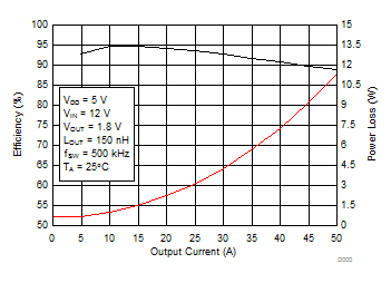
Typical Power Stage Efficiency and Power Loss
