SNAS424D August 2007 – April 2016 DAC088S085
PRODUCTION DATA.
- 1 Features
- 2 Applications
- 3 Description
- 4 Revision History
- 5 Description (continued)
- 6 Pin Configuration and Functions
- 7 Specifications
- 8 Detailed Description
- 9 Application and Implementation
- 10Power Supply Recommendations
- 11Layout
- 12Device and Documentation Support
- 13Mechanical, Packaging, and Orderable Information
Package Options
Mechanical Data (Package|Pins)
Thermal pad, mechanical data (Package|Pins)
- RGH|16
Orderable Information
9 Application and Implementation
NOTE
Information in the following applications sections is not part of the TI component specification, and TI does not warrant its accuracy or completeness. TI’s customers are responsible for determining suitability of components for their purposes. Customers should validate and test their design implementation to confirm system functionality.
9.1 Application Information
9.1.1 Examples Programming the DAC088S085
This section presents the step-by-step instructions for programming the serial input register.
9.1.1.1 Updating DAC Outputs Simultaneously
When the DAC088S085 is first powered on, the DAC is operating in Write Register Mode (WRM). Operating in WRM allows the user to program the registers of multiple DAC channels without causing the DAC outputs to be updated. As an example, here are the steps for setting Channel A to a full scale output, Channel B to three-quarters full scale, Channel C to half-scale, Channel D to one-quarter full scale and having all the DAC outputs update simultaneously.
As stated previously, the DAC088S085 powers up in WRM. If the device was previously operating in Write Through Mode (WTM), an extra step to set the DAC into WRM would be required. First, the DAC registers need to be programmed to the desired values. To set Channel A to an output of full scale, write 0FF0 to the control register. This updates the data register for Channel A without updating the output of Channel A. Second, set Channel B to an output of three-quarters full scale by writing 1C00 to the control register. This updates the data register for Channel B. Once again, the output of Channel B and Channel A is not updated because the DAC is operating in WRM. Third, set Channel C to half scale by writing 2800 to the control register. Fourth, set Channel D to one-quarter full scale by writing 3400 to the control register. Finally, update all four DAC channels simultaneously by writing A00F to the control register. This procedure allows the user to update four channels simultaneously with five steps.
Because Channel A was one of the DACs to be updated, one command step could have been saved by writing to Channel A last. This is accomplished by writing to Channel B, C, and D first and using the special command Channel A Write to update the DAC register and output of Channel A. This special command has the added benefit of updating all DAC outputs while updating Channel A. With this sequence of commands, the user was able to update four channels simultaneously with four steps. A summary of this command can be found in Table 4.
9.1.1.2 Updating DAC Outputs Independently
If the DAC088S085 is currently operating in WRM, change the mode of operation to WTM by writing 9XXX to the control register. Once the DAC is operating in WTM, any DAC channel can be updated in one step. For example, if a design required Channel G to be set to half scale, the user can write 6800 to the control register and the data register of Channel G and DAC output is updated. Similarly, if the output of Channel F needed to be set to full scale, 5FF0 would need to be written to the control register. Channel A is the only channel that has a special command that allows its DAC output to be updated in one command regardless of the mode of operation. Setting the DAC output of Channel A to full scale could be accomplished in one step by writing BFFF to the control register.
9.1.2 Bipolar Operation
The DAC088S085 is designed for single-supply operation and thus has a unipolar output. However, a bipolar output may be achieved with the circuit in Figure 32. This circuit provides an output voltage range of ±5 V. A rail-to-rail amplifier must be used if the amplifier supplies are limited to ±5 V.
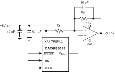 Figure 32. Bipolar Operation
The output voltage of this circuit for any code is found to be
where
- D is the input code in decimal form.
With VA = 5 V and R1 = R2,
A list of rail-to-rail amplifiers suitable for this application are indicated in Table 5.
Table 5. Some Rail-to-Rail Amplifiers
| AMP | PKGS | TYP VOS | TYP ISUPPLY |
|---|---|---|---|
| LMP7701 | SOT-23 | ±37 µV | 0.79 mA |
| LMV841 | SOT-23 | –17 µV | 1.11 mA |
| LMC7111 | SOT-23 | 900 µV | 25 µA |
| LM7301 | SOT-23 | 30 µV | 620 µA |
| LM8261 | SOT-23 | 700 µV | 1 mA |
9.1.3 Variable Current Source Output
The DAC088S085 is a voltage output DAC but can be easily converted to a current output with the addition of an operational amplifier. In Figure 33, one of the channels of the DAC088S085 is converted to a variable current source capable of sourcing up to 40 mA.
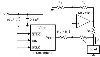 Figure 33. Variable Current Source
The output current of this circuit (IO) for any DAC code is found to be
where
- D is the input code in decimal form
- R2 = RA + RB
9.1.4 DSP and Microprocessor Interfacing
Interfacing the DAC088S085 to microprocessors and DSPs is quite simple. The following guidelines are offered to hasten the design process.
9.1.4.1 ADSP-2101 and ADSP2103 Interfacing
Figure 34 shows a serial interface between the DAC088S085 and the ADSP-2101 or ADSP2103. The DSP must be set to operate in the SPORT Transmit Alternate Framing Mode. It is programmed through the SPORT control register and must be configured for Internal Clock Operation, Active Low Framing and 16-bit Word Length. Transmission is started by writing a word to the Tx register after the SPORT mode has been enabled.
 Figure 34. ADSP-2101 and ADSP-2103 Interface
9.1.4.2 80C51 and 80L51 Interface
A serial interface between the DAC088S085 and the 80C51 or 80L51 microcontroller is shown in Figure 35. The SYNC signal comes from a bit-programmable pin on the microcontroller. The example shown here uses port line P3.3. This line is taken low when data is transmitted to the DAC088S085. Because the 80x51 transmits 8-bit bytes, only eight falling clock edges occur in the transmit cycle. To load data into the DAC, the P3.3 line must be left low after the first eight bits are transmitted. A second write cycle is initiated to transmit the second byte of data, after which port line P3.3 is brought high. The 80x51 transmit routine must recognize that the 80x51 transmits data with the LSB first while the DAC088S085 requires data with the MSB first.
 Figure 35. 80C51 and 80L51 Interface
9.1.4.3 68HC11 Interface
A serial interface between the DAC088S085 and the 68HC11 microcontroller is shown in Figure 36. The SYNC line of the DAC088S085 is driven from a port line (PC7 in the figure), similar to the 80C51 and 80L51.
The 68HC11 must be configured with its CPOL bit as a zero and its CPHA bit as a one. This configuration causes data on the MOSI output to be valid on the falling edge of SCLK. PC7 is taken low to transmit data to the DAC. The 68HC11 transmits data in 8-bit bytes with eight falling clock edges. Data is transmitted with the MSB first. PC7 must remain low after the first eight bits are transferred. A second write cycle is initiated to transmit the second byte of data to the DAC, after which PC7 must be raised to end the write sequence.
 Figure 36. 68HC11 Interface
9.1.4.4 Microwire Interface
Figure 37 shows an interface between a Microwire compatible device and the DAC088S085. Data is clocked out on the rising edges of the SK signal. As a result, the SK of the Microwire device must be inverted before driving the SCLK of the DAC088S085.
 Figure 37. Microwire Interface
9.1.5 Industrial Application
Figure 38 shows the DAC088S085 controlling several different circuits in an industrial setting. Channel A is shown providing the reference voltage to the ADC081S625, one of Texas Instruments' general-purpose Analog-to-Digital Converters (ADCs). The reference for the ADC121S625 may be set to any voltage from 0.2 V to 5.5 V, providing the widest dynamic range possible. Typically, the ADC121S625 is monitoring a sensor and would benefit from the reference voltage of ADC being adjustable. Channel B is providing the drive or supply voltage for a sensor. By having the sensor supply voltage adjustable, the output of the sensor can be optimized to the input level of the ADC monitoring it. Channel C is defined to adjust the offset or gain of an amplifier stage in the system. Channel D is configured with an operational amplifier to provide an adjustable current source. Being able to convert one of the eight channels of the DAC088S085 to a current output eliminates the need for a separate current output DAC to be added to the circuit. Channel E, in conjunction with an operational amplifier, provides a bipolar output swing for devices requiring control voltages that are centered around ground. Channel F and G are used to set the upper and lower limits for a range detector. Channel H is reserved for providing voltage control or acting as a voltage setpoint.
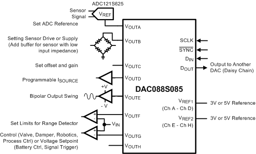 Figure 38. Industrial Application
9.2 Typical Applications
The following figures are examples of the DAC088S085 in typical application circuits. These circuits are basic and generally requires modification for specific circumstances.
9.2.1 ADC Reference
Figure 39 shows Channel A of the DAC088S085 providing the drive or supply voltage for a bridge sensor. By having the sensor supply voltage adjustable, the output of the sensor can be optimized to the input level of the ADC monitoring it.
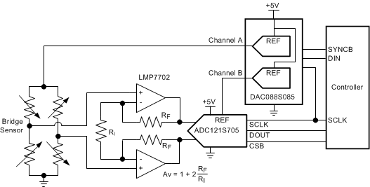 Figure 39. Driving an ADC Reference
9.2.1.1 Design Requirements
For this design example, use these requirements:
- Provide drive for a bridge sensor that is adjustable through SPI from an MCU.
- Provide reference voltage for an ADC that is adjustable through SPI from an MCU.
- Use a single 5 V supply.
- Use ratiometric design for the bridge and ADC reference.
9.2.1.2 Detailed Design Procedure
The output of the sensor is amplified by a fixed gain amplifier stage with a differential gain of 1 + 2 × (RF / RI). The advantage of this amplifier configuration is the high input impedance seen by the output of the bridge sensor. The disadvantage is the poor common-mode rejection ratio (CMRR). The common-mode voltage (VCM) of the bridge sensor is half of the DAC output of Channel A. The VCM is amplified by a gain of 1 V/V by the amplifier stage and thus becomes the bias voltage for the input of the ADC121S705. Channel B of the DAC088S085 is providing the reference voltage to the ADC121S705. The reference for the ADC121S705 may be set to any voltage from 1 V to 5 V, providing the widest dynamic range possible.
The reference voltage for Channel A and B is powered by an external 5 V power supply. Because the 5 V supply is common to the sensor supply voltage and the reference voltage of the ADC, fluctuations in the value of the 5‑V supply has a minimal effect on the digital output code of the ADC. This type of configuration is often referred to as a Ratio-metric design. For example, an increase of 5% to the 5 V supply causes the sensor supply voltage to increase by 5%. This causes the gain or sensitivity of the sensor to increase by 5%. The gain of the amplifier stage is unaffected by the change in supply voltage. The ADC121S705 on the other hand, also experiences a 5% increase to its reference voltage. This causes the size of the least significant bit (LSB) of the ADC to increase by 5%. As a result of the sensor's gain increasing by 5% and the LSB size of the ADC increasing by the same 5%, there is no net effect on the circuit's performance. It is assumed that the amplifier gain is set low enough to allow for a 5% increase in the sensor output. Otherwise, the increase in the sensor output level may cause the output of the amplifiers to clip.
9.2.1.3 Application Curve
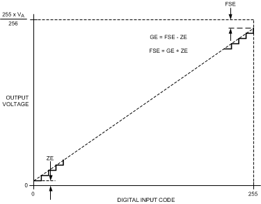 Figure 40. I/O Transfer Characteristic
9.2.2 Programmable Attenuator
Figure 41 shows one of the channels of the DAC088S085 being used as a single-quadrant multiplier.
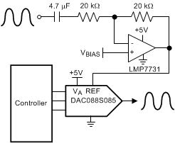 Figure 41. Programmable Attenuator Diagram
9.2.2.1 Design Requirements
For this design example, use these requirements:
- Use a single 5 V supply.
- Use the SPI interface to control the amount of attenuation of a signal.
- Do not add any noise to the signal.
9.2.2.2 Detailed Design Procedure
In this configuration, an AC or DC signal can be driven into one of the reference pins. The SPI interface of the DAC can be used to digitally attenuate the signal to any level from 0 dB (full scale) to 0 V. This is accomplished without adding any noticeable level of noise to the signal. An amplifier stage is shown in Figure 41 as a reference for applications where the input signal requires amplification. Notice how the AC signal in this application is AC-coupled to the amplifier before being amplified. A separate bias voltage is used to set the common-mode voltage for the DAC088S085's reference input to VA / 2, allowing the largest possible input swing. The multiplying bandwidth of VREF1,2 is 360 kHz with a VCM of 2.5 V and a peak-to-peak signal swing of 2 V.
9.2.2.3 Application Curve
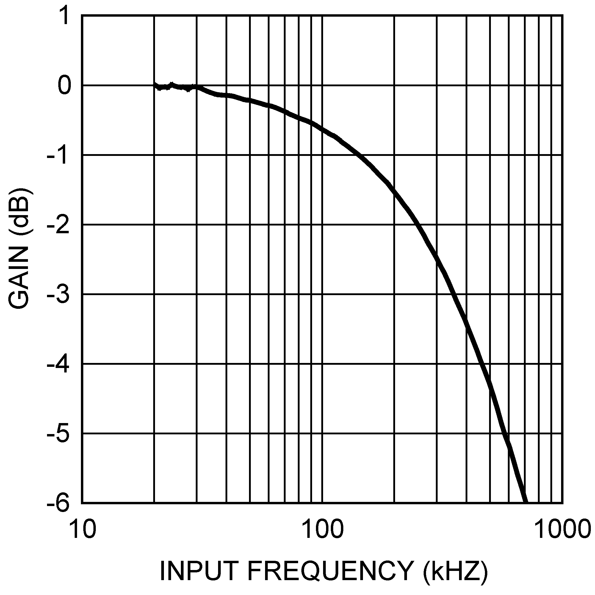 Figure 42. Multiplying Bandwidth
9.3 Do's and Don'ts
- Install bypass capacitors next to the VA, VREF1, and VREF2 pins.
- The reference inputs must be kept stable and noise free. Besides installing bypass capacitors close to the pins, the traces that have the reference voltages must kept away from noisy traces.
- Keep analog and digital traces away from each other. If they need to cross, have the traces cross at a 90° angle.