SNAS424D August 2007 – April 2016 DAC088S085
PRODUCTION DATA.
- 1 Features
- 2 Applications
- 3 Description
- 4 Revision History
- 5 Description (continued)
- 6 Pin Configuration and Functions
- 7 Specifications
- 8 Detailed Description
- 9 Application and Implementation
- 10Power Supply Recommendations
- 11Layout
- 12Device and Documentation Support
- 13Mechanical, Packaging, and Orderable Information
Package Options
Mechanical Data (Package|Pins)
Thermal pad, mechanical data (Package|Pins)
- RGH|16
Orderable Information
11 Layout
11.1 Layout Guidelines
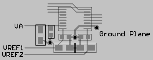
For best accuracy and minimum noise, the printed-circuit board containing the DAC088S085 must have separate analog and digital areas. The areas are defined by the locations of the analog and digital power planes. Both of these planes must be located in the same board layer. A single ground plane is preferred if digital return current does not flow through the analog ground area. Frequently a single ground plane design uses a fencing technique to prevent the mixing of analog and digital ground current. Separate ground planes must only be used when the fencing technique is inadequate. The separate ground planes must be connected in one place, preferably near the DAC088S085. Take special care to ensure that digital signals with fast edge rates do not pass over split ground planes. They must always have a continuous return path below their traces.
For best performance, the DAC088S085 power supply must be bypassed with at least a 1-µF and a 0.1-µF capacitor. The 0.1-µF capacitor must be placed right at the device supply pin. The 1-µF or larger valued capacitor can be a tantalum capacitor while the 0.1-µF capacitor must be a ceramic capacitor with low ESL and low ESR. If a ceramic capacitor with low ESL and low ESR is used for the 1-µF value and it can be placed right at the supply pin, the 0.1-µF capacitor can be eliminated. Capacitors of this nature typically span the same frequency spectrum as the 0.1-µF capacitor and thus eliminate the need for the extra capacitor. The power supply for the DAC088S085 must only be used for analog circuits.
It is also advisable to avoid the crossover of analog and digital signals. This helps minimize the amount of noise from the transitions of the digital signals from coupling onto the sensitive analog signals such as the reference pins and the DAC outputs.
11.2 Layout Example
 Figure 47. Typical Layout