SNVS801B April 2012 – January 2016 DAC101C081 , DAC101C081Q , DAC101C085
PRODUCTION DATA.
- 1 Features
- 2 Applications
- 3 Description
- 4 Revision History
- 5 Description (continued)
- 6 Device Comparison Table
- 7 Pin Configuration and Functions
- 8 Specifications
- 9 Detailed Description
- 10Application and Implementation
- 11Power Supply Recommendations
- 12Layout
- 13Device and Documentation Support
- 14Mechanical, Packaging, and Orderable Information
Package Options
Mechanical Data (Package|Pins)
- NGF|6
Thermal pad, mechanical data (Package|Pins)
Orderable Information
10 Application and Implementation
NOTE
Information in the following applications sections is not part of the TI component specification, and TI does not warrant its accuracy or completeness. TI’s customers are responsible for determining suitability of components for their purposes. Customers should validate and test their design implementation to confirm system functionality.
10.1 Application Information
10.1.1 Bipolar Operation
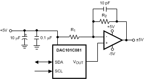
The DAC101C081 is designed for single supply operation and thus has a unipolar output. However, a bipolar output may be obtained with the circuit in Figure 27. This circuit will provide an output voltage range of ±5 Volts. A rail-to-rail amplifier should be used if the amplifier supplies are limited to ±5 V.
 Figure 27. Bipolar Operation
The output voltage of this circuit for any code is found to be:
where
With VA = 5 V and R1 = R2,
A list of rail-to-rail amplifiers suitable for this application are indicated in Table 2.
Table 2. Some Rail-to-Rail Amplifiers
| AMP | PKGS | Typ VOS | Typ ISUPPLY |
|---|---|---|---|
| LMP7701 | SOT-23-5 | 37 uV | 0.79 mA |
| LMV841 | SC70-5 | 50 uV | 1 mA |
| LMC7111 | SOT-23-5 | 0.9 mV | 25 µA |
| LM7301 | SO-8 SOT-23-5 |
0.03 mV | 620 µA |
| LM8261 | SOT-23-5 | 0.7 mV | 1 mA |
10.1.2 DSP/Microprocessor Interfacing
Interfacing the DAC101C081 to microprocessors and DSPs is quite simple. The following guidelines are offered to simplify the design process.
10.1.2.1 Interfacing to the 2-wire Bus
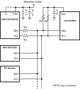
Figure 28 shows a microcontroller interfacing to the DAC101C081 via the 2-wire bus. Pullup resistors (Rp) should be chosen to create an appropriate bus rise time and to limit the current that will be sunk by the open-drain outputs of the devices on the bus. Please refer to the I2C™ Specification for further details. Typical pullup values to use in Standard-Fast mode bus applications are 2kΩ to 10kΩ. SCL and SDA series resisters (RS) near the DAC101C081 are optional. If high-voltage spikes are expected on the 2-wire bus, series resistors should be used to filter the voltage on SDA and SCL. The value of the series resistance must be picked to ensure the VIL threshold can be achieved. If used, RS is typically 51Ω.
 Figure 28. Serial Interface Connection Diagram
10.1.2.2 Interfacing to a Hs-mode Bus
Interfacing to a Hs-mode bus is very similar to interfacing to a standard-fast mode bus. In Hs-mode, the specified rise time of SCL is shortened. To create a faster rise time, the master device (microcontroller) can drive the SCL bus high and low. In other words, the microcontroller can drive the line high rather than leaving it to the pullup resistor. It is also possible to decrease the value of the pullup resistors or increase the pullup current to meet the tighter timing specs. Please refer to the I2C Specification for further details.
10.2 Typical Application
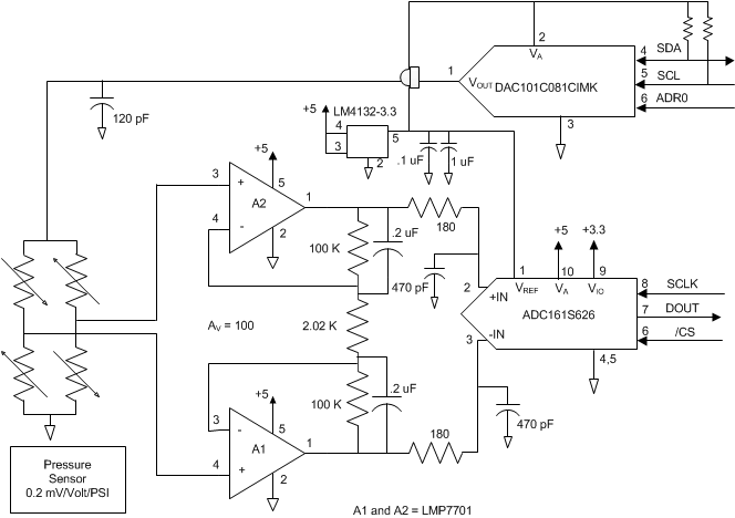
 Figure 29. Pressure Sensor Gain Adjust
10.2.1 Design Requirements
A positive supply only data acquisition system capable of digitizing a pressure sensor output. In addition to digitizing the pressure sensor output, the system designer can use the DAC101C081 to correct for gain errors in the pressure sensor output by adjusting the bias voltage to the bridge pressure sensor.
10.2.2 Detailed Design Procedure
As shown in Equation 4, the output of the pressure sensor is relative to the imbalance of the resistive bridge times the output of the DAC101C081, thus providing the desired gain correction.
Likewise for the ADC161S626, Equation 5 shows that the ADC output is function of the Pressure Sensor Output times relative to the ratio of the ADC input divided by the DAC101C081 output voltage.
10.2.3 Application Curve
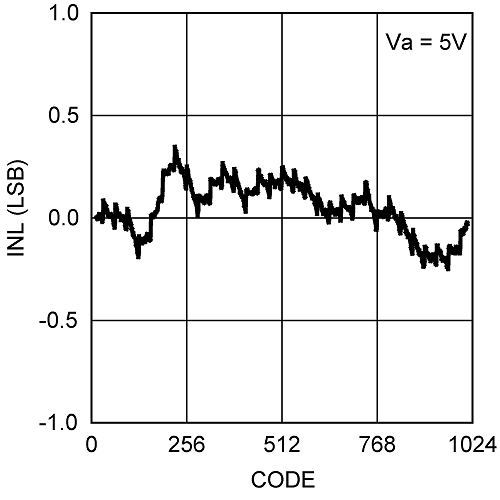
 Figure 30. INL vs Input Code