SNAS321G June 2005 – April 2016 DAC101S101 , DAC101S101-Q1
PRODUCTION DATA.
- 1 Features
- 2 Applications
- 3 Description
- 4 Revision History
- 5 Description (continued)
- 6 Pin Configuration and Functions
- 7 Specifications
- 8 Detailed Description
- 9 Application and Implementation
- 10Power Supply Recommendations
- 11Layout
- 12Device and Documentation Support
- 13Mechanical, Packaging, and Orderable Information
Package Options
Mechanical Data (Package|Pins)
Thermal pad, mechanical data (Package|Pins)
Orderable Information
8 Detailed Description
8.1 Overview
The DAC101S101 is a full-featured, general purpose 10-bit voltage-output digital-to-analog converter (DAC) that can operate from a single +2.7 V to 5.5 V supply and consumes just 175 µA of current at 3.6 Volts. The on-chip output amplifier allows rail-to-rail output swing and the three wire serial interface operates at clock rates up to 30 MHz over the specified supply voltage range and is compatible with standard SPI, QSPI, MICROWIRE and DSP interfaces.
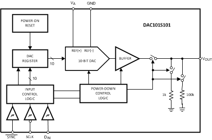
The supply voltage for the DAC101S101 serves as its voltage reference, providing the widest possible output dynamic range. A power-on reset circuit ensures that the DAC output powers up to zero volts and remains there until there is a valid write to the device. A power-down feature reduces power consumption to less than a microWatt.
8.2 Functional Block Diagram

8.3 Feature Description
8.3.1 DAC Section
The DAC101S101 is fabricated on a CMOS process with an architecture that consists of a resistor string and switches that are followed by an output buffer. The power supply serves as the reference voltage. The input coding is straight binary with an ideal output voltage of:
where
- D is the decimal equivalent of the binary code that is loaded into the DAC register and can take on any value between 0 and 1023
8.3.2 Resistor String
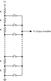
The resistor string is shown in Figure 35. This string consists of 1024 equal valued resistors in series with a switch at each junction of two resistors, plus a switch to ground. The code loaded into the DAC register determines which switch is closed, connecting the proper node to the amplifier. This configuration ensures that the DAC is monotonic.
 Figure 35. DAC Resistor String
8.3.3 Output Amplifier
The output buffer amplifier is a rail-to-rail type, providing an output voltage range of 0V to VA. All amplifiers, even rail-to-rail types, exhibit a loss of linearity as the output approaches the supply rails (0V and VA, in this case). For this reason, linearity is specified over less than the full output range of the DAC. The output capabilities of the amplifier are described in the Electrical Characteristics Tables.
8.3.4 Power-On Reset
The power-on reset circuit controls the output voltage during power-up. The DAC register is filled with zeros and the output voltage is 0 Volts and remains there until a valid write sequence is made to the DAC.
8.4 Device Functional Modes
8.4.1 Power-Down Modes
The DAC101S101 has four modes of operation. These modes are set with two bits (DB13 and DB12) in the control register.
Table 1. Modes of Operation
| DB13 | DB12 | OPERATING MODE |
|---|---|---|
| 0 | 0 | Normal Operation |
| 0 | 1 | Power-Down with 1 kΩ to GND |
| 1 | 0 | Power-Down with 100 kΩ to GND |
| 1 | 1 | Power-Down with Hi-Z |
When both DB13 and DB12 are 0, the device operates normally. For the other three possible combinations of these bits the supply current drops to its power-down level and the output is pulled down with either a 1kΩ or a 100KΩ resistor, or is in a high impedance state, as described in Table 1.
The bias generator, output amplifier, the resistor string and other linear circuitry are all shut down in any of the power-down modes. However, the contents of the DAC register are unaffected when in power-down. Minimum power consumption is achieved in the power-down mode with SCLK disabled and SYNC and DIN idled low. The time to exit power-down (Wake-Up Time) is typically tWU µsec as stated in the A.C. and Timing Requirements Table.
8.5 Programming
8.5.1 Serial Interface
The three-wire interface is compatible with SPI, QSPI and MICROWIRE as well as most DSPs. See the Serial Timing Diagram for information on a write sequence.
A write sequence begins by bringing the SYNC line low. Once SYNC is low, the data on the DIN line is clocked into the 16-bit serial input register on the falling edges of SCLK. On the 16th falling clock edge, the last data bit is clocked in and the programmed function (a change in the mode of operation and/or a change in the DAC register contents) is executed. At this point the SYNC line may be kept low or brought high. In either case, it must be brought high for the minimum specified time before the next write sequence so that a falling edge of SYNC can initiate the next write cycle.
Because the SYNC and DIN buffers draw more current when they are high, they should be idled low between write sequences to minimize power consumption.
8.5.2 Input Shift Register
The input shift register, Figure 36, has sixteen bits. The first two bits are "don't cares" and are followed by two bits that determine the mode of operation (normal mode or one of three power-down modes). The contents of the serial input register are transferred to the DAC register on the sixteenth falling edge of SCLK. See Figure 2.
 Figure 36. Input Register Contents
Normally, the SYNC line is kept low for at least 16 falling edges of SCLK and the DAC is updated on the 16th SCLK falling edge. However, if SYNC is brought high before the 16th falling edge, the shift register is reset and the write sequence is invalid. The DAC register is not updated and there is no change in the mode of operation.
8.5.3 DSP/Microprocessor Interfacing
Interfacing the DAC101S101 to microprocessors and DSPs is quite simple. The following guidelines are offered to hasten the design process.
8.5.3.1 ADSP-2101/ADSP2103 Interfacing
Figure 37 shows a serial interface between the DAC101S101 and the ADSP-2101/ADSP2103. The DSP should be set to operate in the SPORT Transmit Alternate Framing Mode. It is programmed through the SPORT control register and should be configured for Internal Clock Operation, Active Low Framing and 16-bit Word Length. Transmission is started by writing a word to the Tx register after the SPORT mode has been enabled.
 Figure 37. ADSP-2101/2103 Interface
8.5.3.2 80C51/80L51 Interface
A serial interface between the DAC101S101 and the 80C51/80L51 microcontroller is shown in Figure 38. The SYNC signal comes from a bit-programmable pin on the microcontroller. The example shown here uses port line P3.3. This line is taken low when data is to transmitted to the DAC101S101. Since the 80C51/80L51 transmits 8-bit bytes, only eight falling clock edges occur in the transmit cycle. To load data into the DAC, the P3.3 line must be left low after the first eight bits are transmitted. A second write cycle is initiated to transmit the second byte of data, after which port line P3.3 is brought high. The 80C51/80L51 transmit routine must recognize that the 80C51/80L51 transmits data with the LSB first while the DAC101S101 requires data with the MSB first.
 Figure 38. 80C51/80L51 Interface
8.5.3.3 68HC11 Interface
A serial interface between the DAC101S101 and the 68HC11 microcontroller is shown in Figure 39. The SYNC line of the DAC101S101 is driven from a port line (PC7 in the figure), similar to the 80C51/80L51.
The 68HC11 should be configured with its CPOL bit as a zero and its CPHA bit as a one. This configuration causes data on the MOSI output to be valid on the falling edge of SCLK. PC7 is taken low to transmit data to the DAC. The 68HC11 transmits data in 8-bit bytes with eight falling clock edges. Data is transmitted with the MSB first. PC7 must remain low after the first eight bits are transferred. A second write cycle is initiated to transmit the second byte of data to the DAC, after which PC7 should be raised to end the write sequence.
 Figure 39. 68HC11 Interface
8.5.3.4 Microwire Interface
Figure 40 shows an interface between a Microwire compatible device and the DAC101S101. Data is clocked out on the rising edges of the SCLK signal.
 Figure 40. Microwire Interface