-
DAC128S085 12-Bit Micro-Power OCTAL Digital-to-Analog Converter With Rail-to-Rail Outputs
- 1 Features
- 2 Applications
- 3 Description
- 4 Revision History
- 5 Description (continued)
- 6 Pin Configuration and Functions
- 7 Specifications
- 8 Detailed Description
- 9 Application and Implementation
- 10Power Supply Recommendations
- 11Layout
- 12Device and Documentation Support
- 13Mechanical, Packaging, and Orderable Information
- IMPORTANT NOTICE
Package Options
Mechanical Data (Package|Pins)
Thermal pad, mechanical data (Package|Pins)
- RGH|16
Orderable Information
DAC128S085 12-Bit Micro-Power OCTAL Digital-to-Analog Converter With Rail-to-Rail Outputs
1 Features
- Ensured Monotonicity
- Low Power Operation
- Rail-to-Rail Voltage Output
- Daisy-Chain Capability
- Power-on Reset to 0 V
- Simultaneous Output Updating
- Individual Channel Power-Down Capability
- Wide Power Supply Range (2.7 V to 5.5 V)
- Dual Reference Voltages With Range of 0.5 V to VA
- Operating Temperature Range of −40°C to 125°C
- Smallest Package in the Industry
- Resolution 12 Bits
- INL ±8 LSB (Maximum)
- DNL 0.75 / −0.4 LSB (Maximum)
- Settling Time 8.5 μs (Maximum)
- Zero Code Error 15 mV (Maximum)
- Full-Scale Error −0.75 %FSR (Maximum)
- Supply Power
- 1.95 mW (3 V) / 4.85 mW (5 V) Typical
- Power Down 0.3 μW (3 V) / 1 μW (5 V) Typical
2 Applications
- Battery-Powered Instruments
- Digital Gain and Offset Adjustment
- Programmable Voltage and Current Sources
- Programmable Attenuators
- Voltage Reference for ADCs
- Sensor Supply Voltage
- Range Detectors
3 Description
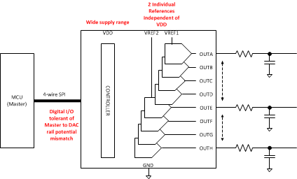
The DAC128S085 is a full-featured, general-purpose OCTAL 12-bit voltage-output digital-to-analog converter (DAC) that can operate from a single 2.7-V to 5.5-V supply and consumes 1.95 mW at 3 V and 4.85 mW at 5 V. The DAC128S085 is packaged in a 16-lead WQFN package and a 16-lead TSSOP package. The WQFN package makes the DAC128S085 the smallest OCTAL DAC in its class. The on-chip output amplifiers allow rail-to-rail output swing, and the 3-wire serial interface operates at clock rates up to 40 MHz over the entire supply voltage range. Competitive devices are limited to 25-MHz clock rates at supply voltages in the 2.7-V to 3.6-V range. The serial interface is compatible with standard SPI™, QSPI, MICROWIRE, and DSP interfaces. The DAC128S085 also offers daisy-chain operation, where an unlimited number of DAC128S085s can be updated simultaneously using a single serial interface.
There are two references for the DAC128S085. One reference input serves channels A through D, while the other reference serves channels E through H. Each reference can be set independently between 0.5 V and VA, providing the widest possible output dynamic range. The DAC128S085 has a 16-bit input shift register that controls the mode of operation, the power-down condition, and the register/output value of the DAC channels. All eight DAC outputs can be updated simultaneously or individually.
Device Information(1)
| PART NUMBER | PACKAGE | BODY SIZE (NOM) |
|---|---|---|
| DAC128S085 | TSSOP (16) | 5.00 mm × 4.4 mm |
| WQFN (16) | 4.00 mm × 4.00 mm |
- For all available packages, see the orderable addendum at the end of the datasheet.
Simplified Schematic
4 Revision History
Changes from G Revision (January 2015) to H Revision
- Switched WQFN and TSSOP pinouts to their correct titles Go
- Re-drew TSSOP pinout as a square to better reflect mechanical packaging drawings Go
Changes from F Revision (March 2013) to G Revision
- Added Pin Configuration and Functions section, ESD Ratings table, Feature Description section, Device Functional Modes, Application and Implementation section, Power Supply Recommendations section, Layout section, Device and Documentation Support section, and Mechanical, Packaging, and Orderable Information section Go
Changes from E Revision (March 2013) to F Revision
- Changed layout of National Data Sheet to TI formatGo
5 Description (continued)
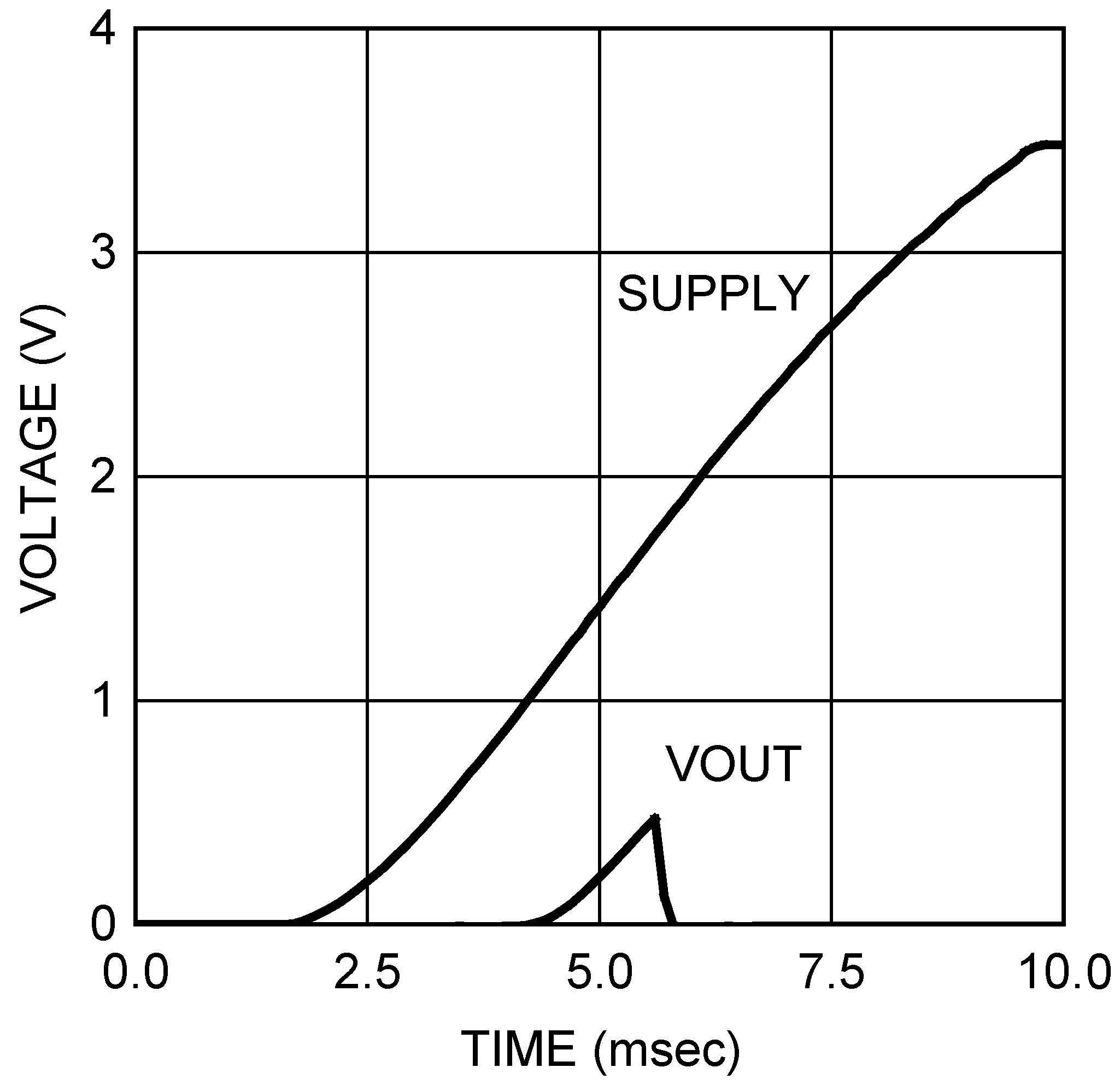
A power-on reset circuit ensures that the DAC outputs power up to zero volts and remain there until there is a valid write to the device. The power-down feature of the DAC128S085 allows each DAC to be independently powered with three different termination options. With all the DAC channels powered down, power consumption reduces to less than 0.3 µW at 3 V and less than 1 µW at 5 V. The low power consumption and small packages of the DAC128S085 make it an excellent choice for use in battery-operated equipment.
The DAC128S085 is one of a family of pin-compatible DACs, including the 8-bit DAC088S085 and the 10-bit DAC108S085. All three parts are offered with the same pinout, allowing system designers to select a resolution appropriate for their application without redesigning their printed circuit board. The DAC128S085 operates over the extended industrial temperature range of −40°C to 125°C.
6 Pin Configuration and Functions


Pin Functions
7 Specifications
7.1 Absolute Maximum Ratings
over operating free-air temperature range (unless otherwise noted)(1)(1)| MIN | MAX | UNIT | ||
|---|---|---|---|---|
| Supply Voltage, VA | 6.5 | V | ||
| Voltage on any Input Pin | −0.3 | 6.5 | V | |
| Input Current at Any Pin(2) | 10 | mA | ||
| Package Input Current(2) | 30 | mA | ||
| Power Consumption at TA = 25°C | See (3) | |||
| Junction Temperature | 150 | °C | ||
| Storage Temperature, Tstg | −65 | 150 | °C | |
7.2 ESD Ratings
| VALUE | UNIT | |||
|---|---|---|---|---|
| V(ESD) | Electrostatic discharge | Human body model (HBM), per ANSI/ESDA/JEDEC JS-001(1) | ±2500 | V |
| Charged-device model (CDM), per JEDEC specification JESD22-C101(2) | ±1000 | |||
| Machine Model | ±250 | |||
7.3 Recommended Operating Conditions
over operating free-air temperature range (unless otherwise noted)| MIN | MAX | UNIT | ||
|---|---|---|---|---|
| Operating Temperature Range | −40 ≤ TA ≤ +125 | °C | ||
| Supply Voltage, VA | 2.7 | 5.5 | V | |
| Reference Voltage, VREF1,2 | 0.5 | VA | V | |
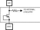
| Digital Input Voltage(1) | 0.0 | 5.5 | V | |
| Output Load | 0 | 1500 | pF | |
| SCLK Frequency | 40 | MHz | ||
7.4 Thermal Information
| THERMAL METRIC(1) | DAC128S085 | UNIT | ||
|---|---|---|---|---|
| PW (TSSOP) | RGH (WQFN) | |||
| 16 PINS | 16 PINS | |||
| RθJA | Junction-to-ambient thermal resistance | 98 | 34 | °C/W |
| RθJA | Junction-to-ambient thermal resistance | 31 | 25 | |
| RθJA | Junction-to-ambient thermal resistance | 43 | 11 | |
| φJT | Junction-to-top characterization parameter | 2 | 0.2 | |
| φJB | Junction-to-board characterization parameter | 43 | 11 | |
7.5 Electrical Characteristics
The following specifications apply for VA = 2.7 V to 5.5 V, VREF1 = VREF2 = VA, CL = 200 pF to GND, fSCLK = 30 MHz, input code range 48 to 4047. All limits are at TA = 25°C, unless otherwise specified.| PARAMETER | TEST CONDITIONS | MIN(2) | TYP | MAX(2) | UNIT | ||
|---|---|---|---|---|---|---|---|
| STATIC PERFORMANCE | |||||||
| Resolution | TMIN ≤ TA ≤ TMAX | 12 | Bits | ||||
| Monotonicity | TMIN ≤ TA ≤ TMAX | 12 | Bits | ||||
| INL | Integral Non-Linearity | ±2 | LSB | ||||
| TMIN ≤ TA ≤ TMAX | ±8 | ||||||
| DNL | Differential Non-Linearity | 0.15 | LSB | ||||
| TMIN ≤ TA ≤ TMAX | 0.75 | ||||||
| −0.09 | LSB | ||||||
| TMIN ≤ TA ≤ TMAX | −0.4 | ||||||
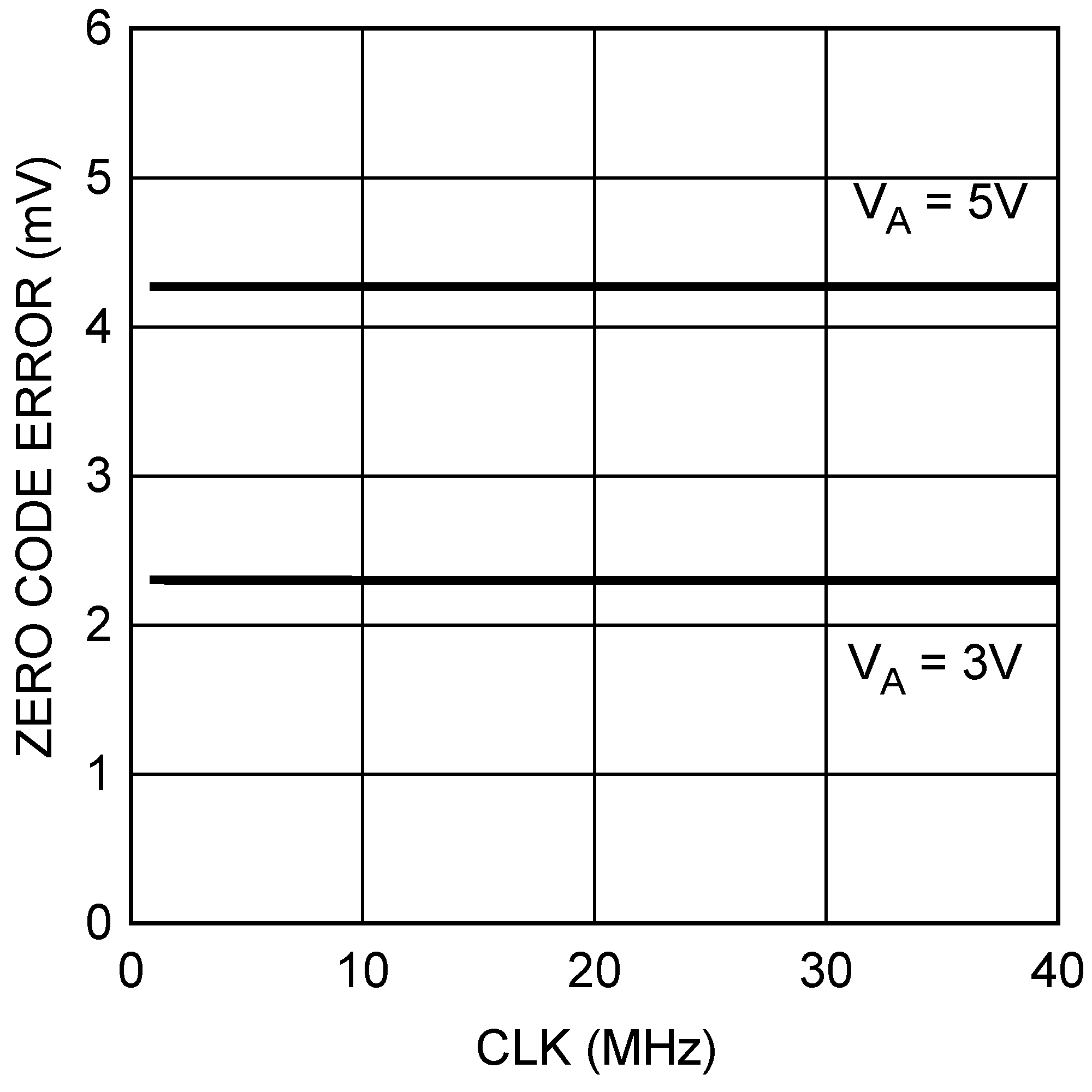
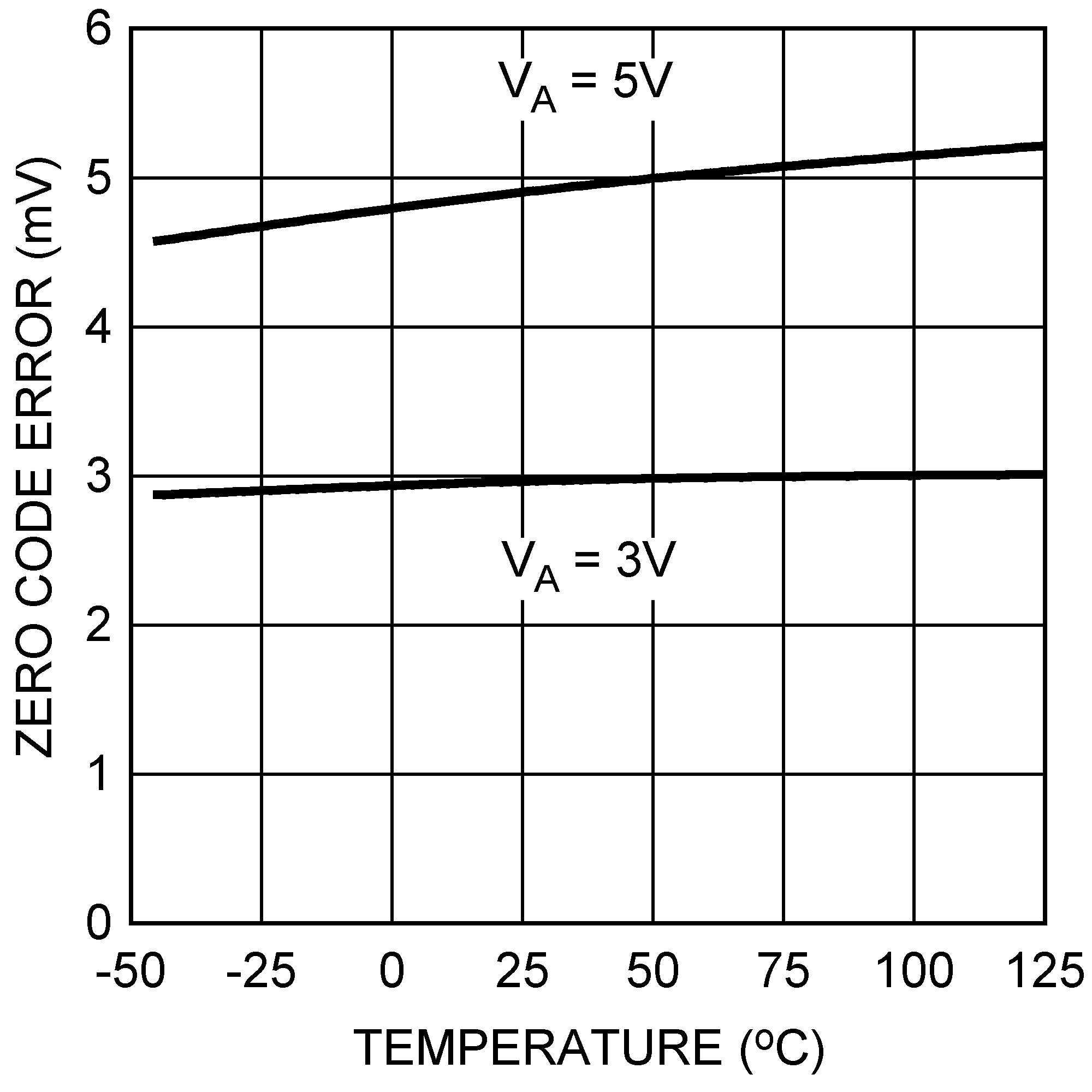
| ZE | Zero Code Error | IOUT = 0 | +5 | mV | |||
| TMIN ≤ TA ≤ TMAX | 15 | ||||||
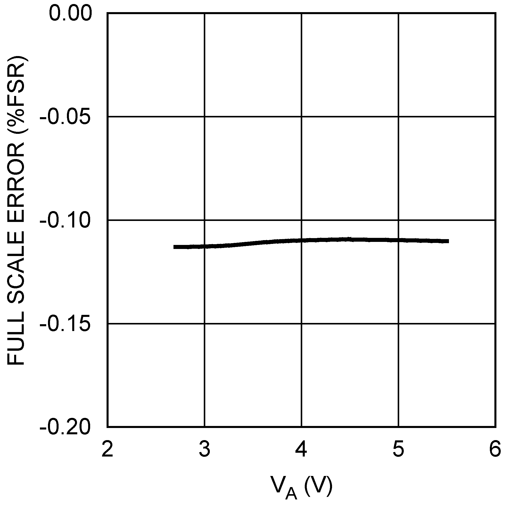
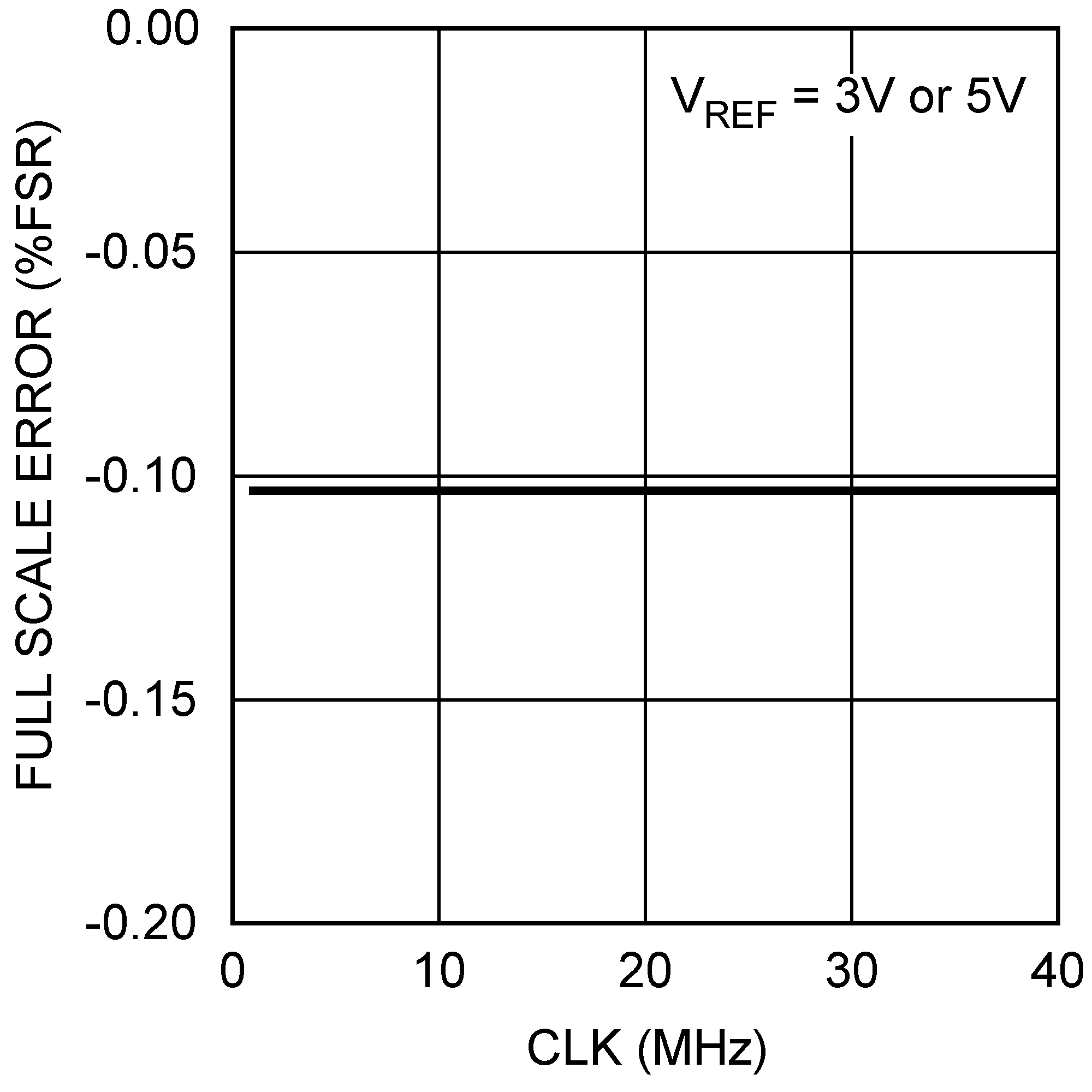
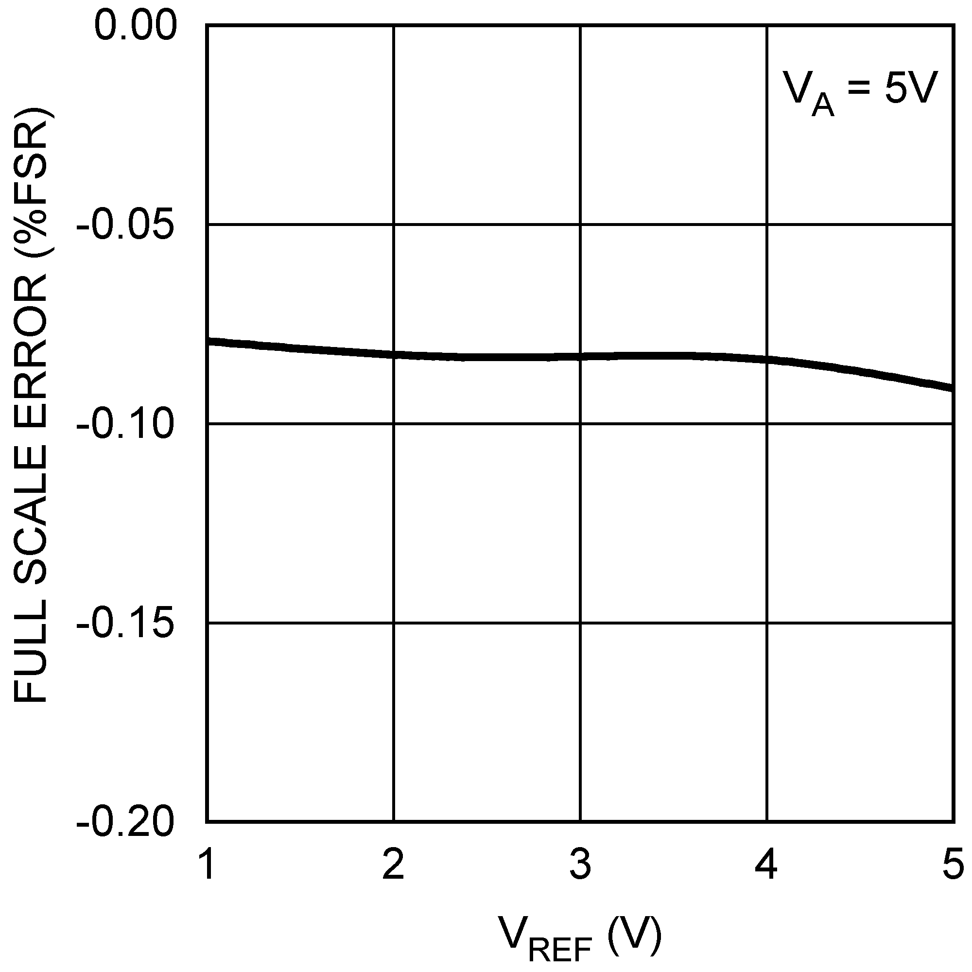
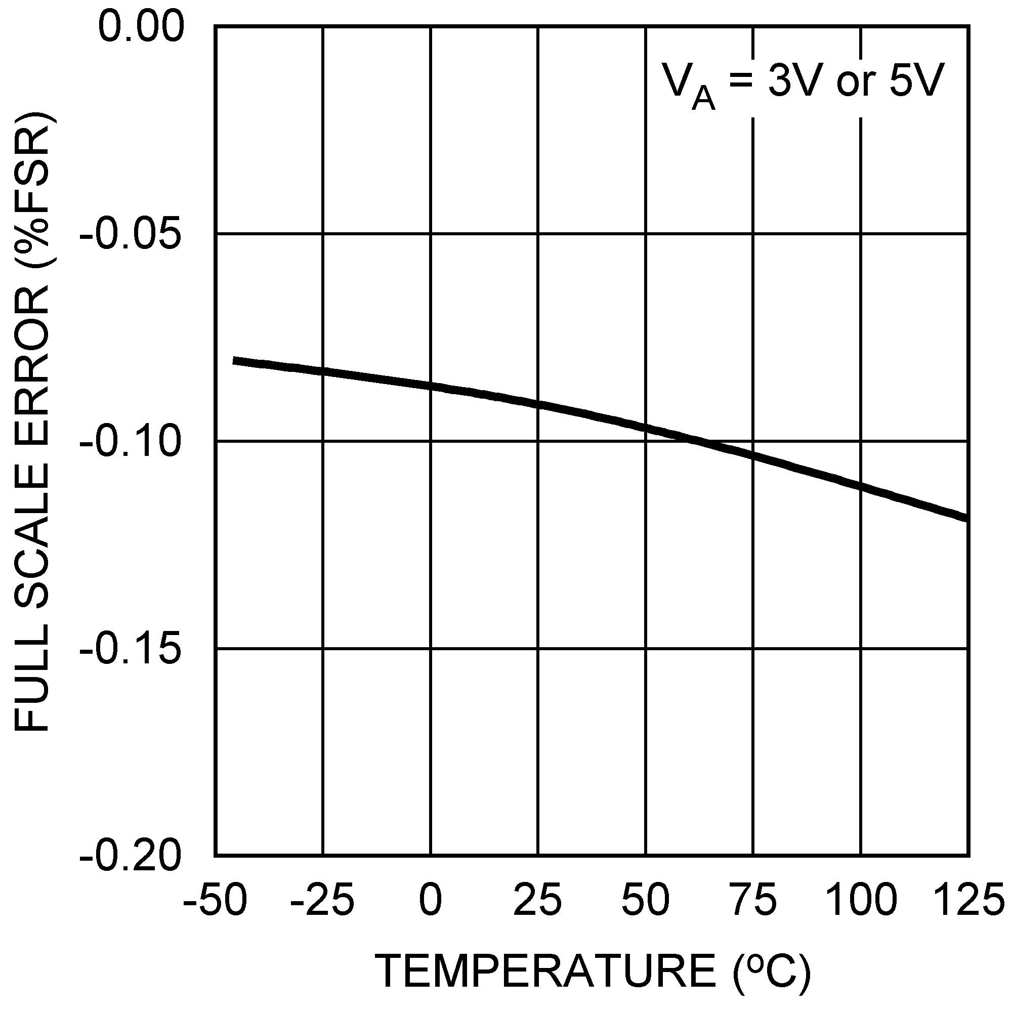
| FSE | Full-Scale Error | IOUT = 0 | −0.1% | FSR | |||
| TMIN ≤ TA ≤ TMAX | −0.75% | ||||||
| GE | Gain Error | −0.2% | FSR | ||||
| TMIN ≤ TA ≤ TMAX | −1 % | ||||||
| ZCED | Zero Code Error Drift | −20 | µV/°C | ||||
| TC GE | Gain Error Tempco | −1 | ppm/°C | ||||
| OUTPUT CHARACTERISTICS | |||||||
| Output Voltage Range | TMIN ≤ TA ≤ TMAX | 0 | VREF1,2 | V | |||
| IOZ | High-Impedance Output Leakage Current(3) |
TMIN ≤ TA ≤ TMAX | ±1 | µA | |||
| ZCO | Zero Code Output | VA = 3 V, IOUT = 200 µA | 10 | mV | |||
| VA = 3 V, IOUT = 1 mA | 45 | mV | |||||
| VA = 5 V, IOUT = 200 µA | 8 | mV | |||||
| VA = 5 V, IOUT = 1 mA | 34 | mV | |||||
| FSO | Full Scale Output | VA = 3 V, IOUT = 200 µA | 2.984 | V | |||
| VA = 3 V, IOUT = 1 mA | 2.933 | V | |||||
| VA = 5 V, IOUT = 200 µA | 4.987 | V | |||||
| VA = 5 V, IOUT = 1 mA | 4.955 | V | |||||
| IOS | Output Short Circuit Current (source)(4) | VA = 3 V, VOUT = 0 V, Input Code = FFFh |
−50 | mA | |||
| VA = 5 V, VOUT = 0 V, Input Code = FFFh |
−60 | mA | |||||
| IOS | Output Short Circuit Current (sink)(4) | VA = 3 V, VOUT = 3 V, Input Code = 000h |
50 | mA | |||
| VA = 5 V, VOUT = 5 V, Input Code = 000h |
70 | mA | |||||
| IO | Continuous Output Current per channel(3) | TA = 105°C TMIN ≤ TA ≤ TMAX |
10 | mA | |||
| TA = 125°C TMIN ≤ TA ≤ TMAX |
6.5 | mA | |||||
| CL | Maximum Load Capacitance | RL = ∞ | 1500 | pF | |||
| RL = 2 kΩ | 1500 | pF | |||||
| ZOUT | DC Output Impedance | 8 | Ω | ||||
| REFERENCE INPUT CHARACTERISTICS | |||||||
| VREF1,2 | Input Range Minimum | 0.5 | V | ||||
| TMIN ≤ TA ≤ TMAX | 2.7 | ||||||
| Input Range Maximum | TMIN ≤ TA ≤ TMAX | VA | V | ||||
| Input Impedance | 30 | kΩ | |||||
| LOGIC INPUT CHARACTERISTICS | |||||||
| IIN | Input Current(3) | TMIN ≤ TA ≤ TMAX | ±1 | µA | |||
| VIL | Input Low Voltage | VA = 2.7 V to 3.6 V | 1 | V | |||
| TMIN ≤ TA ≤ TMAX | 0.6 | ||||||
| VA = 4.5 V to 5.5 V | 1.1 | V | |||||
| 0.8 | |||||||
| VIH | Input High Voltage | VA = 2.7 V to 3.6 V | 1.4 | V | |||
| TMIN ≤ TA ≤ TMAX | 2.1 | ||||||
| VA = 4.5 V to 5.5 V | 2 | V | |||||
| TMIN ≤ TA ≤ TMAX | 2.4 | ||||||
| CIN | Input Capacitance(3) | TMIN ≤ TA ≤ TMAX | 3 | pF | |||
| POWER REQUIREMENTS | |||||||
| VA | Supply Voltage Minimum | TMIN ≤ TA ≤ TMAX | 2.7 | V | |||
| Supply Voltage Maximum | TMIN ≤ TA ≤ TMAX | 5.5 | V | ||||
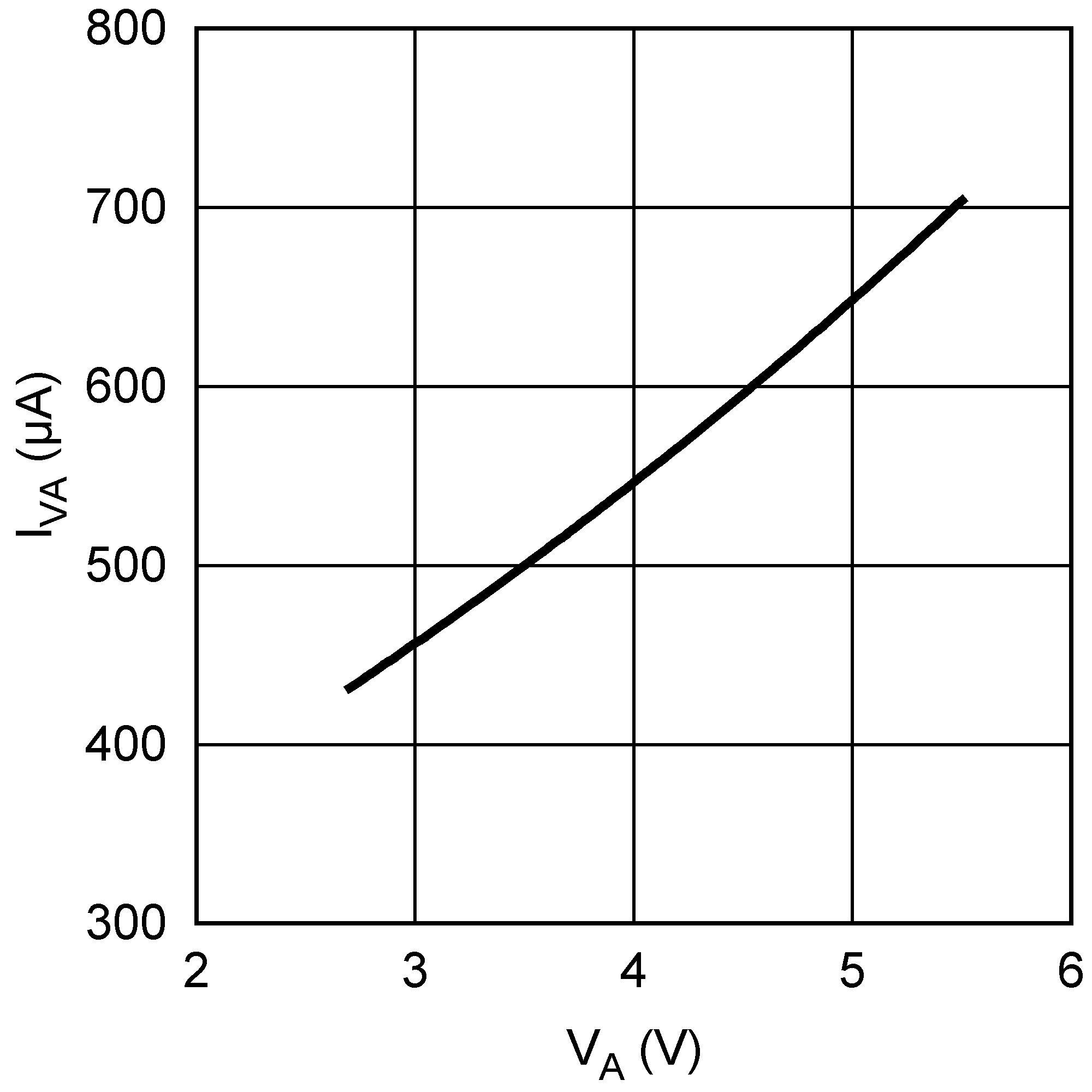
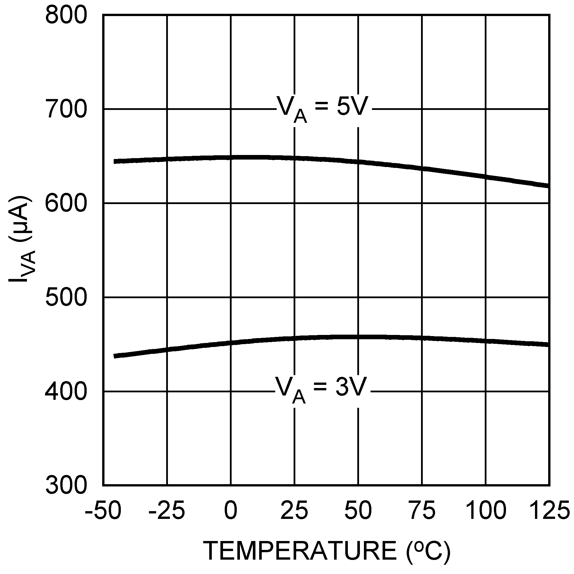
| IN | Normal Supply Current for supply pin VA | fSCLK = 30 MHz, output unloaded |
VA = 2.7 V to 3.6 V | 460 | µA | ||
| TMIN ≤ TA ≤ TMAX | 560 | ||||||
| VA = 4.5 V to 5.5 V | 650 | µA | |||||
| 830 | |||||||
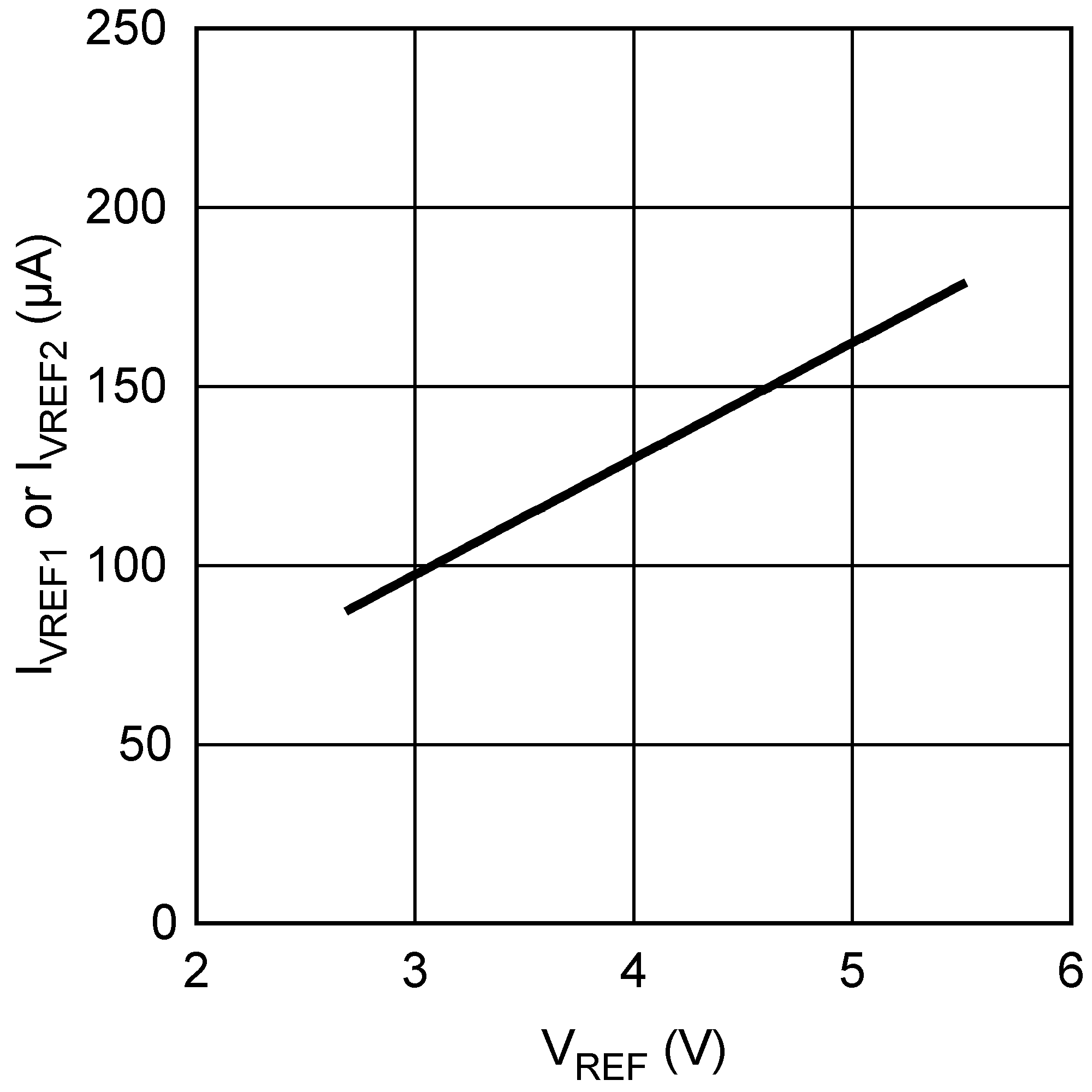
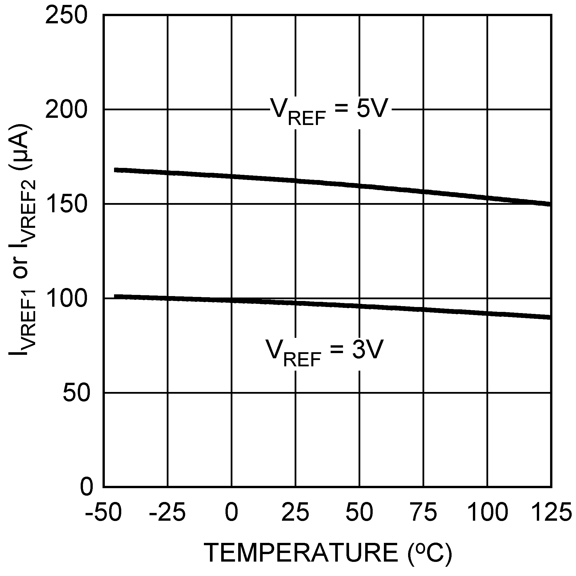
| Normal Supply Current for VREF1 or VREF2 | fSCLK = 30 MHz, output unloaded |
VA = 2.7 V to 3.6 V | 95 | µA | |||
| TMIN ≤ TA ≤ TMAX | 130 | ||||||
| VA = 4.5 V to 5.5 V | 160 | µA | |||||
| 220 | |||||||
| IST | Static Supply Current for supply pin VA | fSCLK = 0, output unloaded |
VA = 2.7 V to 3.6 V | 370 | µA | ||
| VA = 4.5 V to 5.5 V | 440 | µA | |||||
| Static Supply Current for VREF1 or VREF2 | fSCLK = 0, output unloaded |
VA = 2.7 V to 3.6 V | 95 | µA | |||
| VA = 4.5 V to 5.5 V | 160 | µA | |||||
| IPD | Total Power Down Supply Current for all PD Modes (3) |
fSCLK = 30 MHz, SYNC = VA and DIN = 0V after PD mode loaded | VA = 2.7 V to 3.6 V | 0.2 | µA | ||
| 1.5 | |||||||
| VA = 4.5 V to 5.5 V | 0.5 | µA | |||||
| TMIN ≤ TA ≤ TMAX | 3 | ||||||
| fSCLK = 0, SYNC = VA and DIN = 0V after PD mode loaded | VA = 2.7 V to 3.6 V | 0.1 | µA | ||||
| TMIN ≤ TA ≤ TMAX | 1 | ||||||
| VA = 4.5 V to 5.5 V | 0.2 | µA | |||||
| TMIN ≤ TA ≤ TMAX | 2 | ||||||
| PN | Total Power Consumption (output unloaded) | fSCLK = 30 MHz output unloaded |
VA = 2.7 V to 3.6 V | 1.95 | mW | ||
| TMIN ≤ TA ≤ TMAX | 3 | ||||||
| VA = 4.5 V to 5.5 V | 4.85 | mW | |||||
| TMIN ≤ TA ≤ TMAX | 7 | ||||||
| fSCLK = 0 output unloaded |
VA = 2.7 V to 3.6 V | 1.68 | mW | ||||
| VA = 4.5 V to 5.5 V | 3.80 | mW | |||||
| PPD | Total Power Consumption in all PD Modes, (3) |
fSCLK = 30 MHz, SYNC = VA and DIN = 0V after PD mode loaded | VA = 2.7 V to 3.6 V | 0.6 | µW | ||
| TMIN ≤ TA ≤ TMAX | 5.4 | ||||||
| VA = 4.5V to 5.5V | 2.5 | µW | |||||
| TMIN ≤ TA ≤ TMAX | 16.5 | ||||||
| fSCLK = 0, SYNC = VA and DIN = 0V after PD mode loaded | VA = 2.7 V to 3.6 V | 0.3 | µW | ||||
| TMIN ≤ TA ≤ TMAX | 3.6 | ||||||
| VA = 4.5 V to 5.5 V | 1 | µW | |||||
| TMIN ≤ TA ≤ TMAX | 11 | ||||||
7.6 AC and Timing Characteristics
The following specifications apply for VA = 2.7 V to 5.5 V, VREF1,2 = VA, CL = 200 pF to GND, fSCLK = 30 MHz, input code range 48 to 4047. All limits are at TA = 25°C, unless otherwise specified.| MIN(2) | NOM | MAX(2) | UNIT | ||||
|---|---|---|---|---|---|---|---|
| fSCLK | SCLK Frequency | 40 | MHz | ||||
| TMIN ≤ TA ≤ TMAX | 30 | ||||||
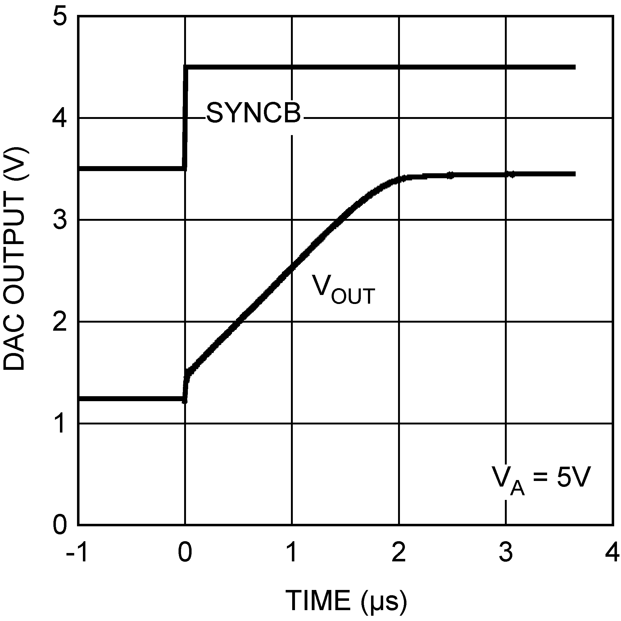
| ts | Output Voltage Settling Time (3) |
400h to C00h code change RL = 2 kΩ, CL = 200 pF |
6 | µs | |||
| TMIN ≤ TA ≤ TMAX | 8.5 | ||||||
| SR | Output Slew Rate | 1 | V/µs | ||||
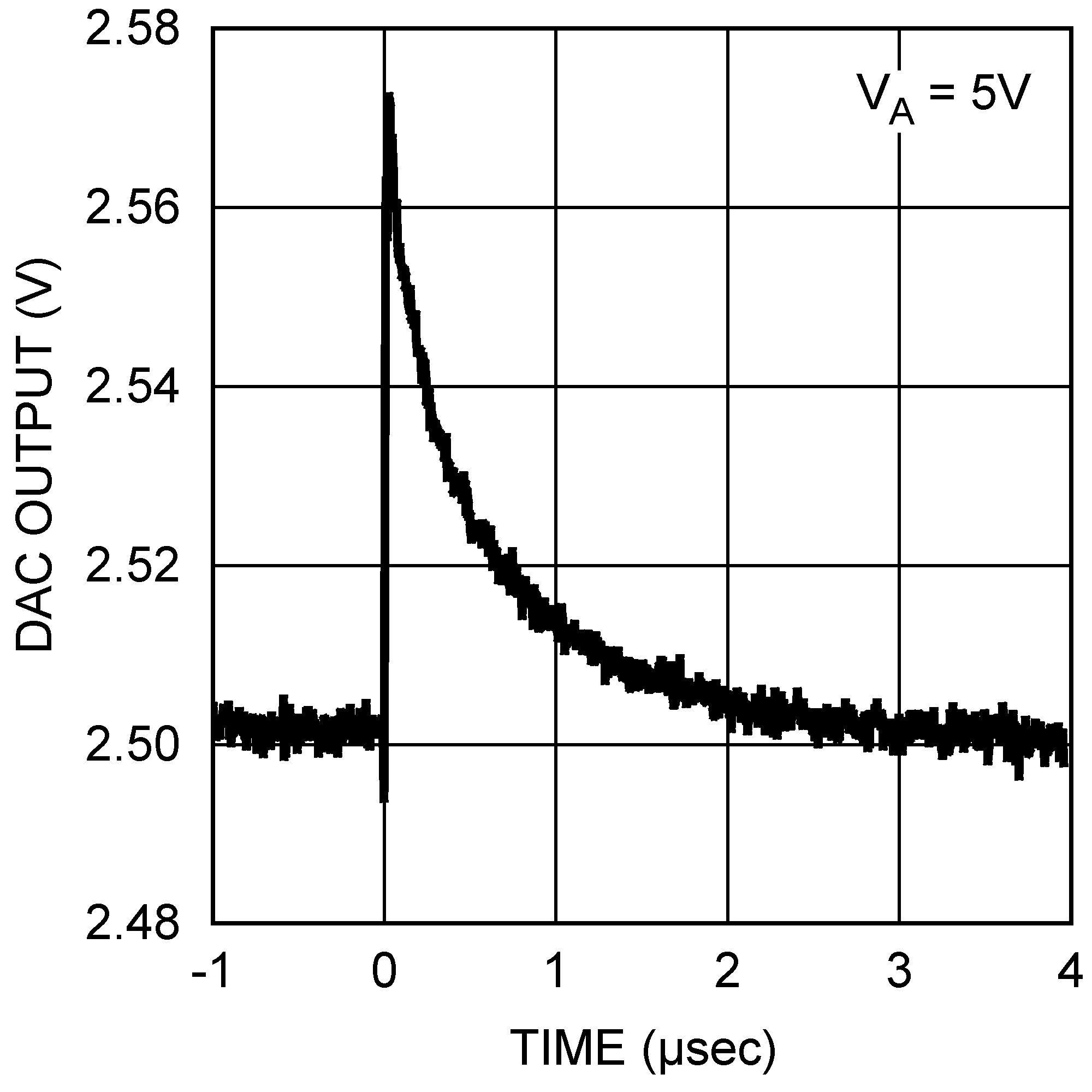
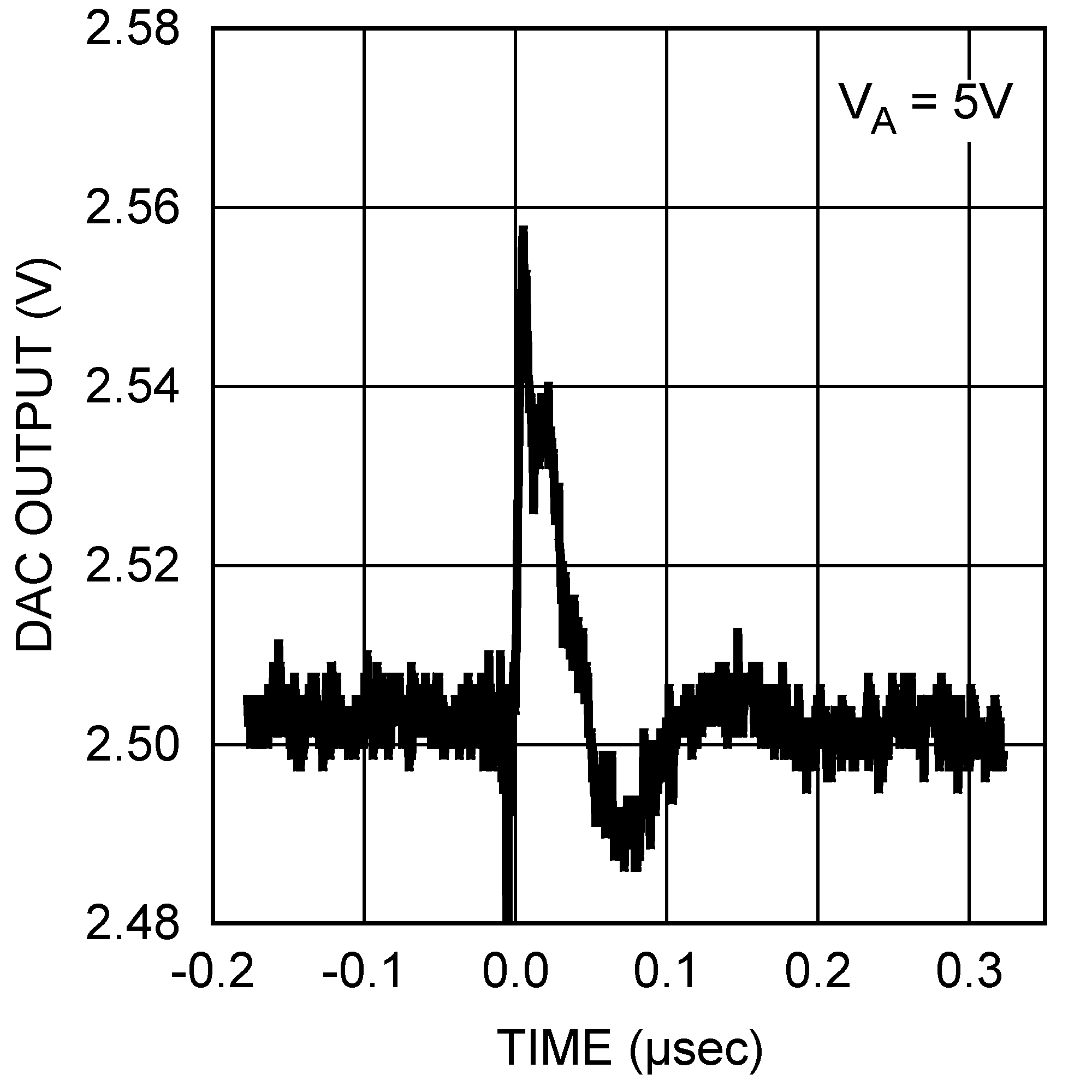
| GI | Glitch Impulse | Code change from 800h to 7FFh | 40 | nV-sec | |||
| DF | Digital Feedthrough | 0.5 | nV-sec | ||||
| DC | Digital Crosstalk | 0.5 | nV-sec | ||||
| CROSS | DAC-to-DAC Crosstalk | 1 | nV-sec | ||||
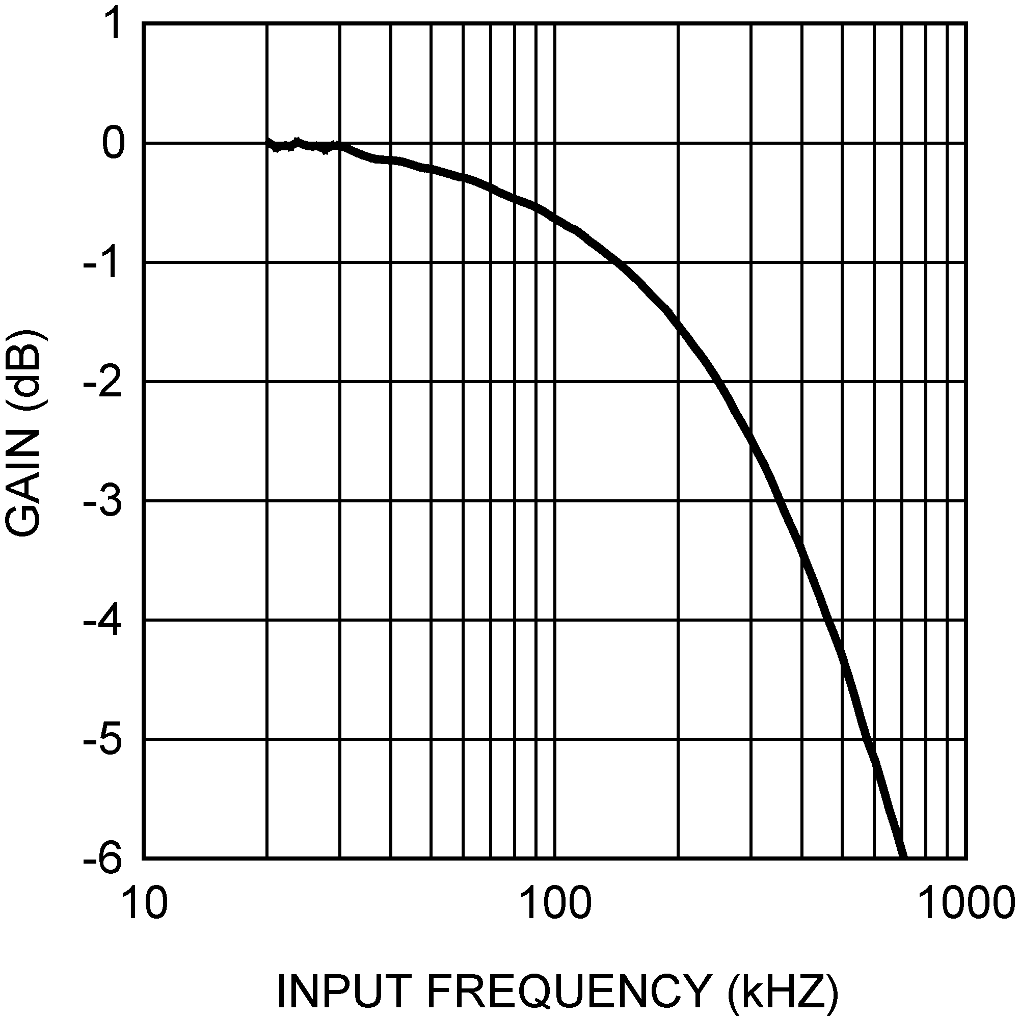
| MBW | Multiplying Bandwidth | VREF1,2 = 2.5 V ± 2 Vpp | 360 | kHz | |||
| THD+N | Total Harmonic Distortion Plus Noise | VREF1,2 = 2.5 V ± 0.5 Vpp 100 Hz < fIN < 20 kHz |
−80 | dB | |||
| ONSD | Output Noise Spectral Density | DAC Code = 800 h, 10 kHz | 40 | nV/sqrt (Hz) | |||
| ON | Output Noise | BW = 30 kHz | 14 | µV | |||
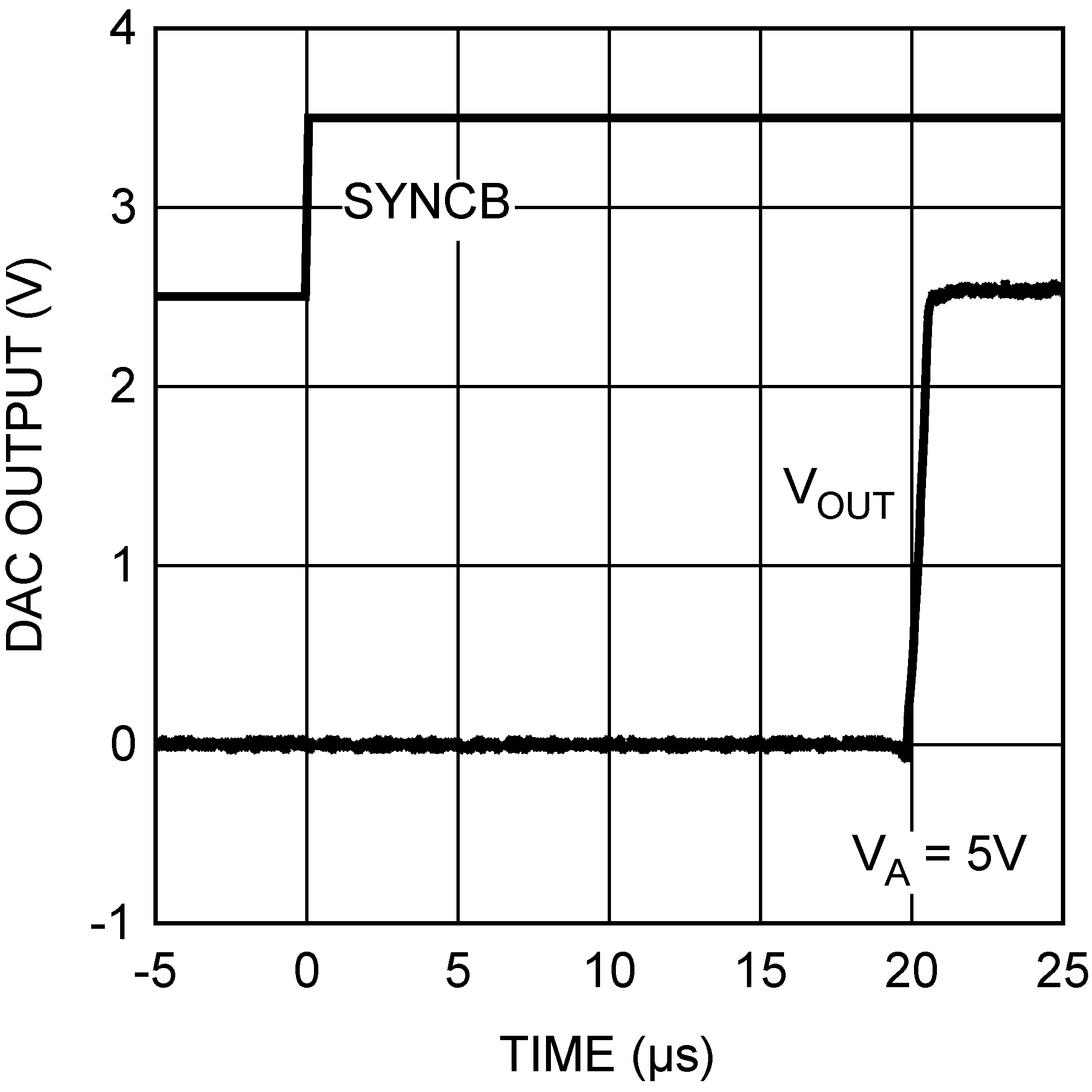
| tWU | Wake-Up Time | VA = 3 V | 3 | µsec | |||
| VA = 5 V | 20 | µsec | |||||
| 1/fSCLK | SCLK Cycle Time. See Figure 1 | 25 | ns | ||||
| TMIN ≤ TA ≤ TMAX | 33 | ||||||
| tCH | SCLK High time. See Figure 1 | 7 | ns | ||||
| TMIN ≤ TA ≤ TMAX | 10 | ||||||
| tCL | SCLK Low Time. See Figure 1 | 7 | ns | ||||
| TMIN ≤ TA ≤ TMAX | 10 | ||||||
| tSS | SYNC Set-up Time prior to SCLK Falling Edge. See Figure 1 | 3 | 1 / fSCLK - 3 | ns | |||
| TMIN ≤ TA ≤ TMAX | 10 | ||||||
| tDS | Data Set-Up Time prior to SCLK Falling Edge. See Figure 1 | 1 | ns | ||||
| TMIN ≤ TA ≤ TMAX | 2.5 | ||||||
| tDH | Data Hold Time after SCLK Falling Edge. See Figure 1 | 1 | ns | ||||
| TMIN ≤ TA ≤ TMAX | 2.5 | ||||||
| tSH | SYNC Hold Time after the 16th falling edge of SCLK. See Figure 1 | 0 | 1 / fSCLK - 3 | ns | |||
| TMIN ≤ TA ≤ TMAX | 3 | ||||||
| tSYNC | SYNC High Time. See Figure 1 | 5 | ns | ||||
| TMIN ≤ TA ≤ TMAX | 15 | ||||||
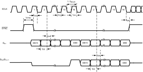 Figure 1. Serial Timing Diagram
7.7 Typical Characteristics
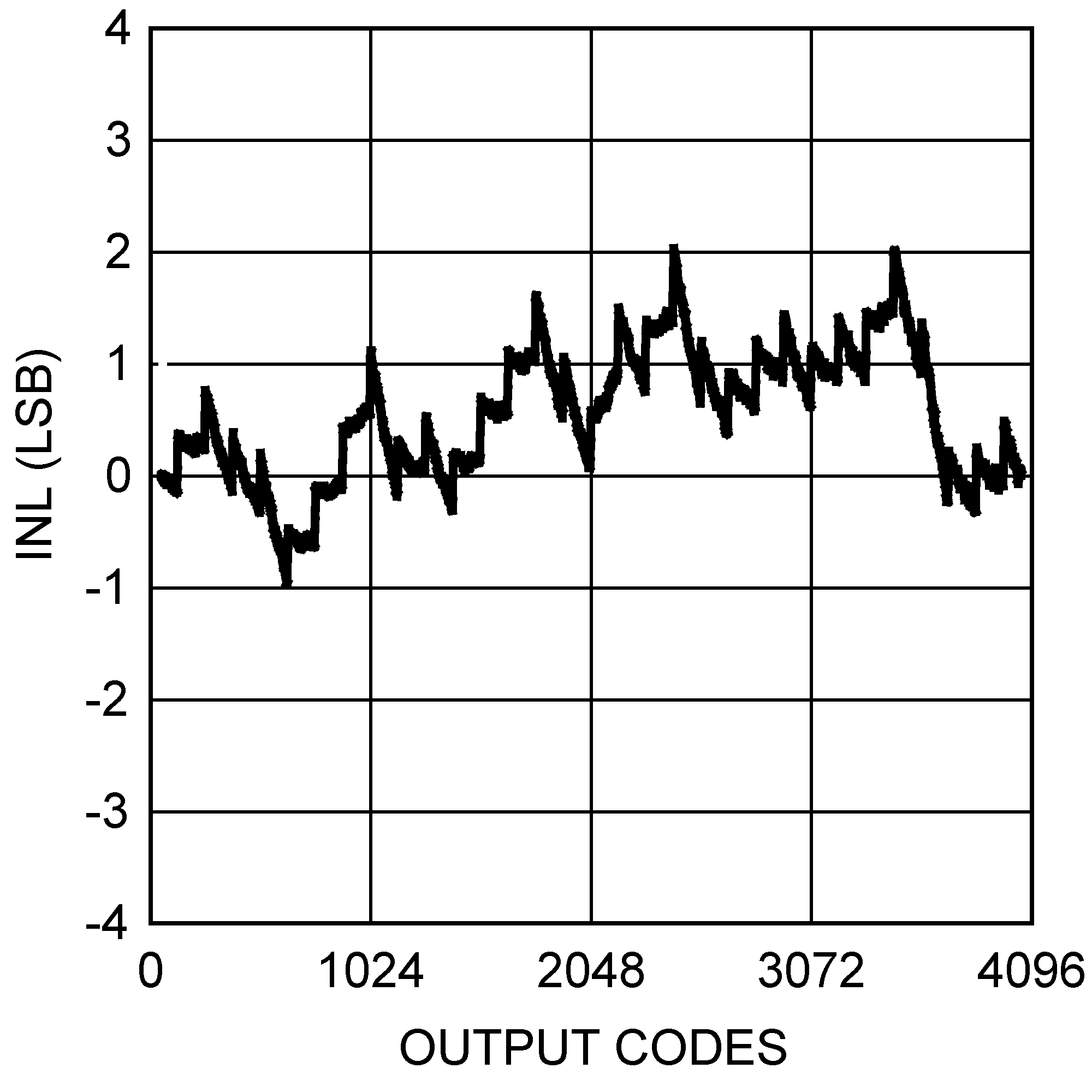
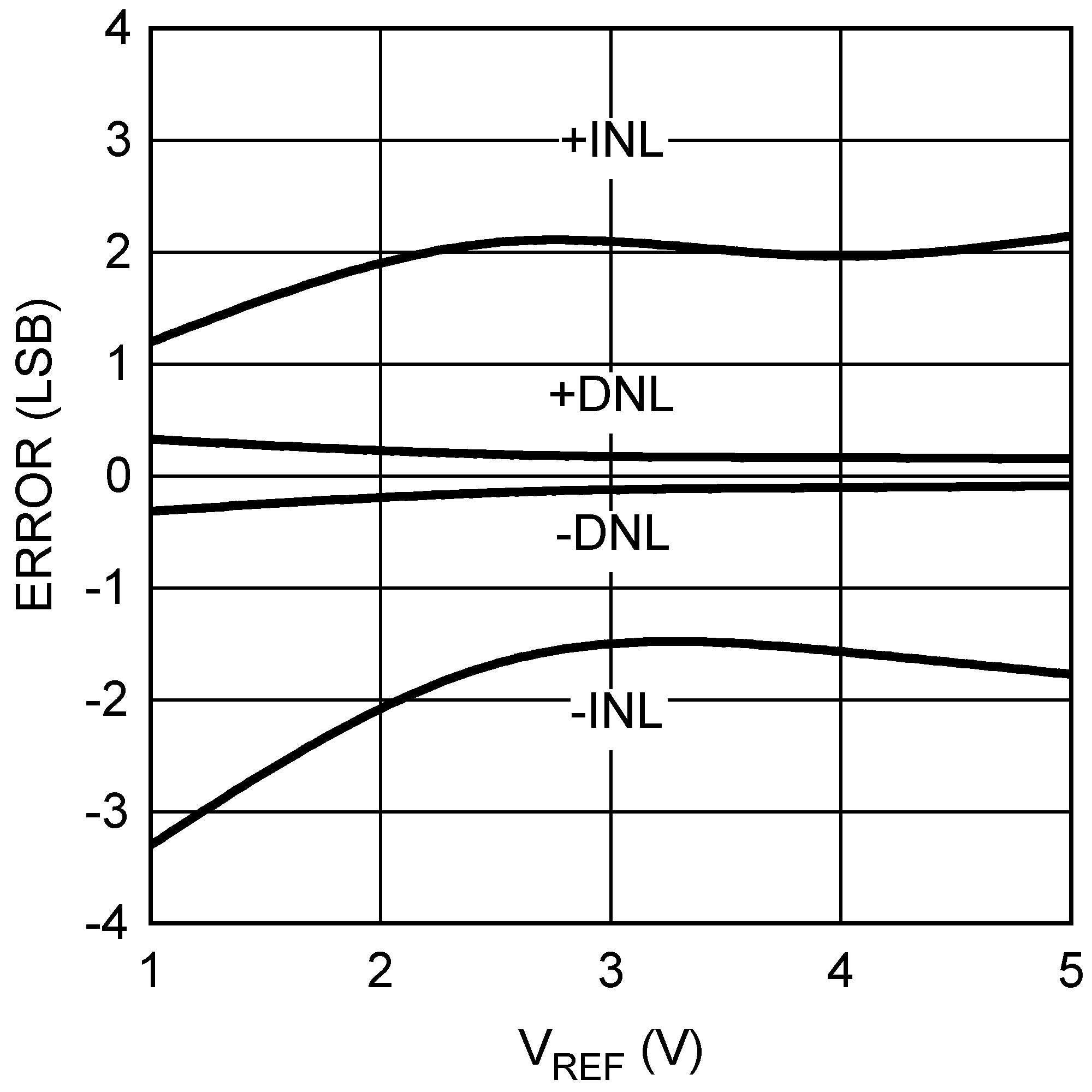
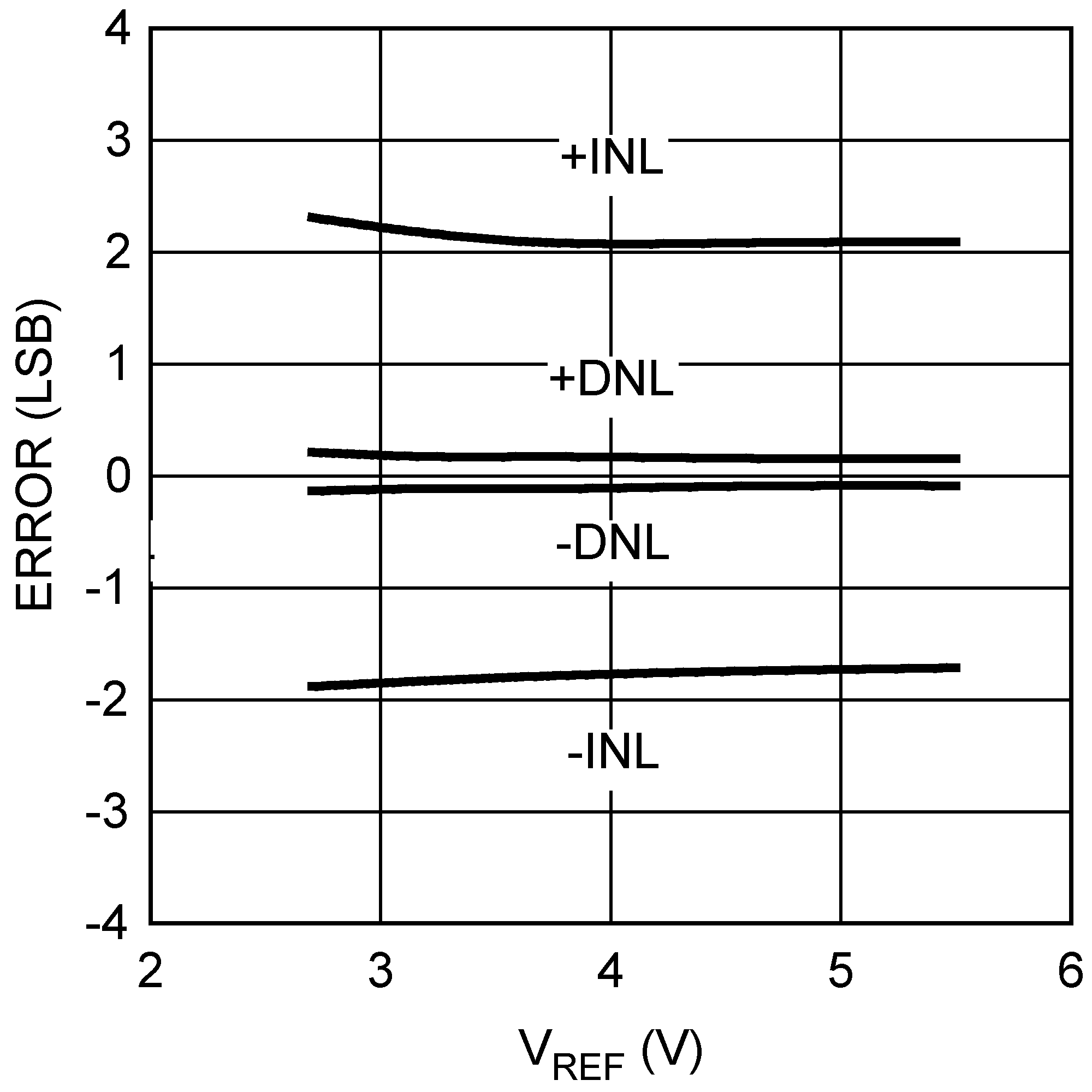
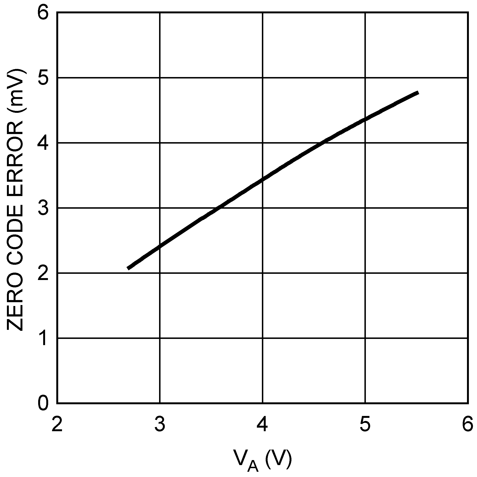
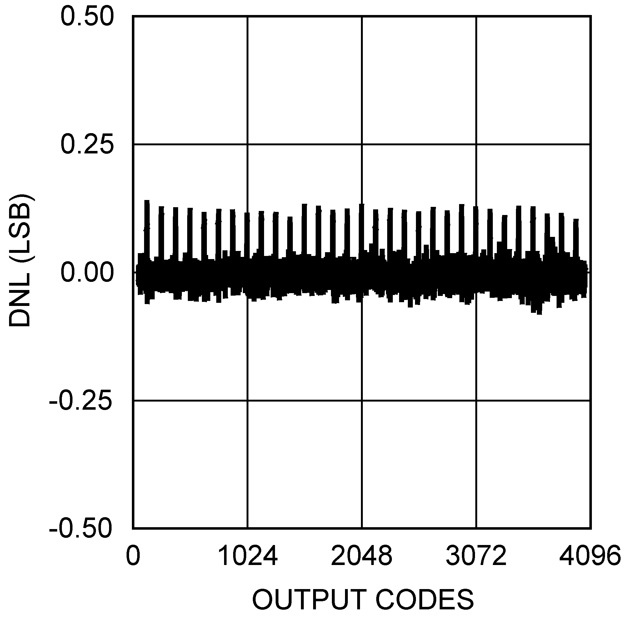
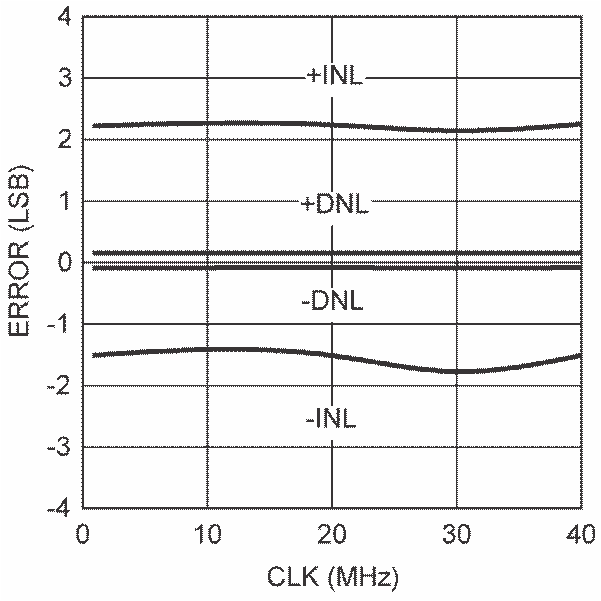
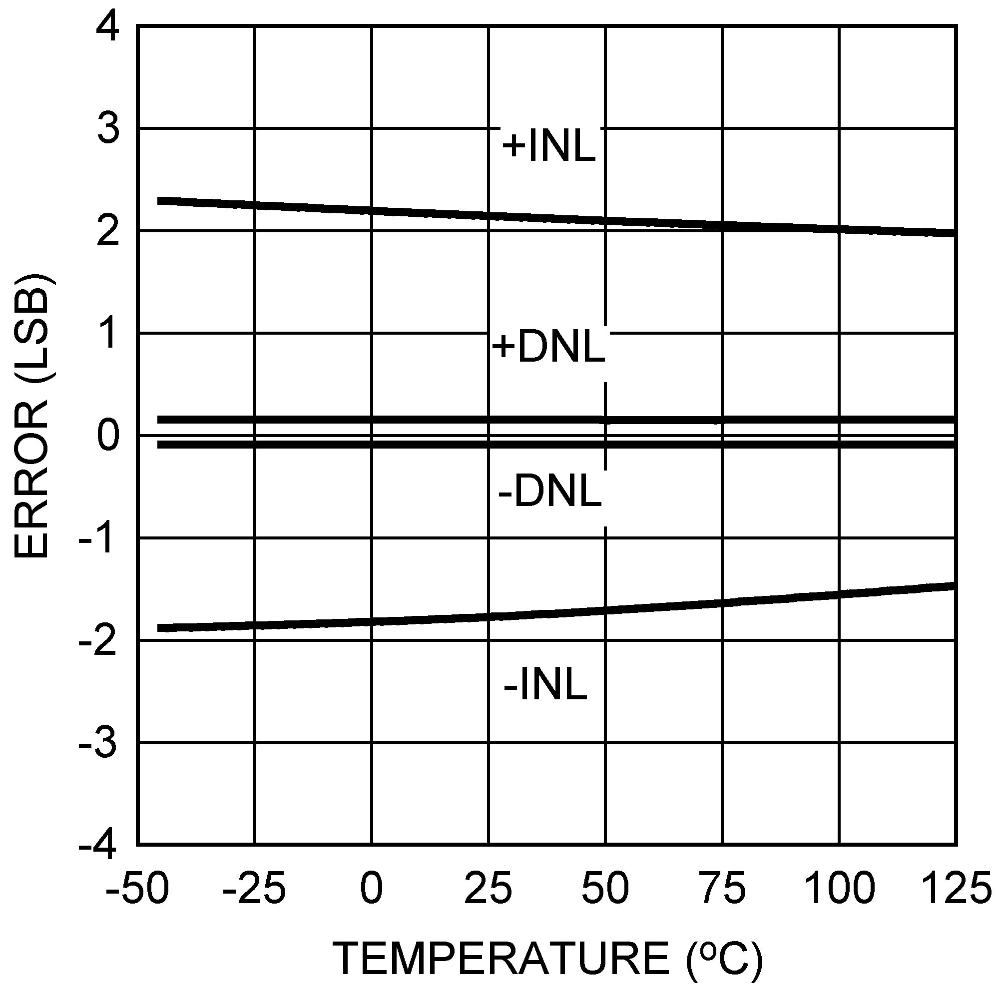
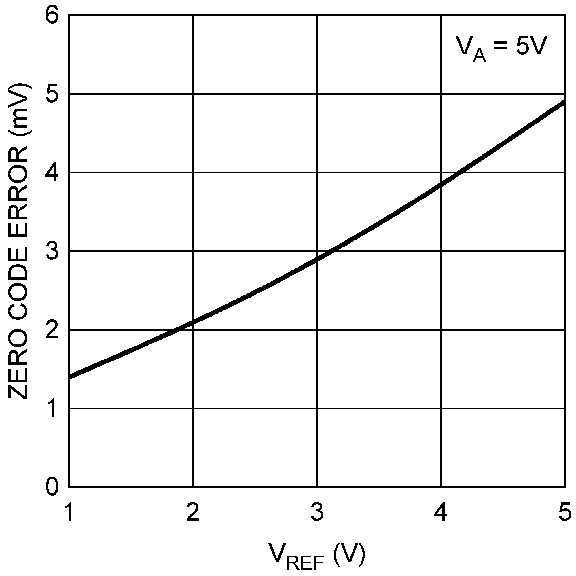
VA = 2.7 V to 5.5 V, VREF1,2 = VA, fSCLK = 30 MHz, TA = 25°C, unless otherwise stated