SBAS932 March 2024 DAC39RF10-SEP , DAC39RF10-SP , DAC39RFS10-SEP , DAC39RFS10-SP
PRODMIX
- 1
- 1 Features
- 2 Applications
- 3 Description
- 4 Device Comparison
- 5 Pin Configuration and Functions
-
6 Specifications
- 6.1 Absolute Maximum Ratings
- 6.2 ESD Ratings
- 6.3 Recommended Operating Conditions
- 6.4 Thermal Information
- 6.5 Electrical Characteristics - DC Specifications
- 6.6 Electrical Characteristics - AC Specifications
- 6.7 Electrical Characteristics - Power Consumption
- 6.8 Timing Requirements
- 6.9 Switching Characteristics
- 6.10 SPI and FRI Timing Diagrams
- 6.11 Typical Characteristics: Bandwidth and DC Linearity
- 6.12 Typical Characteristics: Single Tone Spectra
- 6.13 Typical Characteristics: Dual Tone Spectra
- 6.14 Typical Characteristics: Noise Spectral Density
- 6.15 Typical Characteristics: Power Dissipation and Supply Currents
- 6.16 Typical Characteristics: Linearity Sweeps
- 6.17 Typical Characteristics: Modulated Waveforms
- 6.18 Typical Characteristics: Phase and Amplitude Noise
-
7 Detailed Description
- 7.1 Overview
- 7.2 Functional Block Diagrams
- 7.3
Feature Description
- 7.3.1 DAC Output Modes
- 7.3.2 DAC Core
- 7.3.3 DEM and Dither
- 7.3.4 Offset Adjustment
- 7.3.5 Clocking Subsystem
- 7.3.6 Digital Signal Processing Blocks
- 7.3.7
JESD204C Interface
- 7.3.7.1 Deviation from JESD204C Standard
- 7.3.7.2 Transport Layer
- 7.3.7.3 Scrambler and Descrambler
- 7.3.7.4 Link Layer
- 7.3.7.5 Physical Layer
- 7.3.7.6 Serdes PLL Control
- 7.3.7.7 Serdes Crossbar
- 7.3.7.8 Multi-Device Synchronization and Deterministic Latency
- 7.3.7.9 Operation in Subclass 0 Systems
- 7.3.7.10 Link Reset
- 7.3.8 Alarm Generation
- 7.4 Device Functional Modes
- 7.5 Programming
-
8 Application and Implementation
- 8.1 Application Information
- 8.2 Typical Application
- 8.3 Power Supply Recommendations
- 8.4 Layout
- 9 Device and Documentation Support
- 10Revision History
- 11Mechanical, Packaging, and Orderable Information
Package Options
Mechanical Data (Package|Pins)
- ACL|256
Thermal pad, mechanical data (Package|Pins)
Orderable Information
7.5.2 Using the Fast Reconfiguration Interface
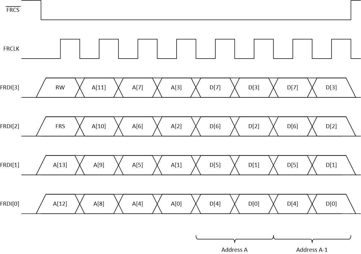
The FR interface provides fast write-only access to configure NCO frequencies and synchronization. The FR interface is similar to the SPI interface, but 4 bits are sent per clock cycle. The FR timing diagram is shown in Figure 7-60. It uses a R/W bit (always Write for this device), a transaction sync bit (FRS), and 14-bits of address followed by some number of data bytes. The address is decremented after each data byte (consistent with little-endian). The interface is byte addressable and data is committed after each byte. The FR interface is takes 4-bits (one nibble) per clock. For multi-nibble fields, data is sent most-significant nibble first. When the transaction sync bit (FRS) is set, the synchronization event specified in the NCO_SYNC_SRC register field occurs at the rising edge of FRCS. Transactions ended before the completion of the first data byte may not trigger the sync event.
 Figure 7-60 FR Interface Timing Diagram
The FR interface registers are listed in Table 7-44. There are two registers that can change the NCO frequency - FR_FREQL[3:0] is 64-bits for each NCO and changes the entire frequency word. FR_FREQS[3:0] is 32-bits for each NCO and changes only the upper 32-bits of the frequency word, providing for faster frequency changes.
| Address | Name | Description |
|---|---|---|
| 0x00FF | FR_NCO_AR | FR NCO Accumulator Reset (default: 0x0f) [7:4] RESERVED [3:0] FR_NCO_AR For each bit FR_NCO_AR[n], if set, the accumulator for NCOn is reset on every sync event specified by NCO_SYNC_SRC. Note: This register has no effect when FR_EN=0. |
| 0x0100-0x011F | FR_FREQL[3:0] | FR 64-bit Frequency for NCO Accumulator (default for FR_FREQL[n]=0x00) The frequency setting for FR_FREQL[0] is at the lowest address. [63:0] FR_FREQL[n] This register is used instead of FREQ[n] when FR_EN=1. Changes to the upper 32-bits of this register also change FR_FREQS[n]. Note: Changes to this register do not take effect until the next sync event specified by NCO_SYNC_SRC. Note: This register has no effect when FR_EN=0. |
| 0x0120-0x0127 | FR_PHASE[3:0] | FR Phase for NCO Accumulator (default for FR_PHASE[n]=0x0000) The phase setting for FR_PHASE[0] is at the lowest address. [15:0] FR_PHASE[n] This register is used instead of PHASE[n] when FR_EN=1. Note: Changes to this register do not take effect until the next sync event specified by NCO_SYNC_SRC. Note: This register has no effect when FR_EN=0. |
| 0x0128-0x0137 | FR_FREQS[3:0] | FR 32-bit Frequency for NCO Accumulator (default for FR_FREQS[n]=0x00) The frequency setting for FR_FREQS[0] is at the lowest address. [31:0] FR_FREQS[n] This register is used instead of FREQ[n] when FR_EN=1. Changes to this register also change the upper 32-bits of FR_FREQL[n]. This register only controls the upper 32-bits of the frequency. The lower 32-bits of the frequency are always controlled by FR_FREQL[n]. Note: Changes to this register do not take effect until the next sync event specified by NCO_SYNC_SRC. Note: This register has no effect when FR_EN=0. |