SLASF08A December   2021  – May 2024 DAC43508 , DAC53508 , DAC63508

PRODUCTION DATA  

  1.   1
  2. Features
  3. Applications
  4. Description
  5. Pin Configurations and Functions
  6. Specifications
    1. 5.1  Absolute Maximum Ratings
    2. 5.2  ESD Ratings
    3. 5.3  Recommended Operating Conditions
    4. 5.4  Thermal Information
    5. 5.5  Electrical Characteristics
    6. 5.6  Timing Requirements: SPI
    7. 5.7  Timing Requirements: Logic
    8. 5.8  Timing Diagrams
    9. 5.9  Typical Characteristics: Static Performance
    10. 5.10 Typical Characteristics: Dynamic Performance
    11. 5.11 Typical Characteristics: General
  7. Detailed Description
    1. 6.1 Overview
    2. 6.2 Functional Block Diagram
    3. 6.3 Feature Description
      1. 6.3.1 Digital-to-Analog Converter (DAC) Architecture
        1. 6.3.1.1 DAC Transfer Function
        2. 6.3.1.2 DAC Register Update and LDAC Functionality
        3. 6.3.1.3 CLR Functionality
        4. 6.3.1.4 Output Amplifier
      2. 6.3.2 Reference
      3. 6.3.3 Power-On Reset (POR)
      4. 6.3.4 Software Reset
    4. 6.4 Device Functional Modes
      1. 6.4.1 Power-Down Mode
    5. 6.5 Programming
      1. 6.5.1 Serial Peripheral Interface (SPI)
  8. Register Map
    1. 7.1 DEVICE_CONFIG Register (address = 01h) [reset = 00FFh]
    2. 7.2 STATUS_TRIGGER Register (address = 02h) [reset = 0000h]
    3. 7.3 BRDCAST Register (address = 03h) [reset = 0000h]
    4. 7.4 DACn_DATA Register (address = 08h to 0Fh) [reset = 0000h]
  9. Application and Implementation
    1. 8.1 Application Information
    2. 8.2 Typical Applications
      1. 8.2.1 Programmable LED Biasing
        1. 8.2.1.1 Design Requirements
        2. 8.2.1.2 Detailed Design Procedure
        3. 8.2.1.3 Application Curve
      2. 8.2.2 Programmable Window Comparator
        1. 8.2.2.1 Design Requirements
        2. 8.2.2.2 Detailed Design Procedure
        3. 8.2.2.3 Application Curve
    3. 8.3 Power Supply Recommendations
    4. 8.4 Layout
      1. 8.4.1 Layout Guidelines
      2. 8.4.2 Layout Example
  10. Device and Documentation Support
    1. 9.1 Documentation Support
      1. 9.1.1 Related Documentation
    2. 9.2 Receiving Notification of Documentation Updates
    3. 9.3 Support Resources
    4. 9.4 Trademarks
    5. 9.5 Electrostatic Discharge Caution
    6. 9.6 Glossary
  11. 10Revision History
  12. 11Mechanical, Packaging, and Orderable Information

Package Options

Refer to the PDF data sheet for device specific package drawings

Mechanical Data (Package|Pins)
  • RTE|16
Thermal pad, mechanical data (Package|Pins)
Orderable Information

Application Curve

DAC43508 DAC53508 DAC63508 DC
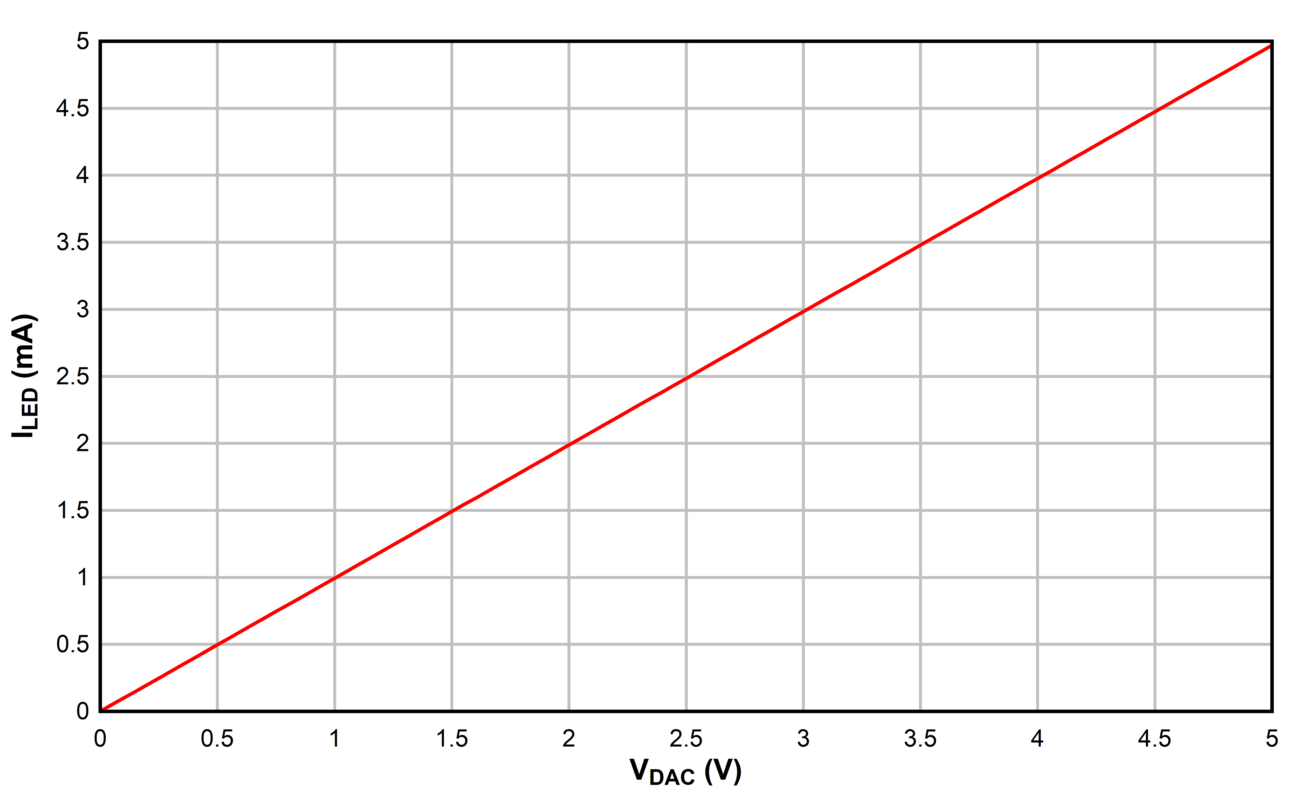
                        Transfer Characteristics of LED Biasing Circuit
Figure 8-2 DC Transfer Characteristics of LED Biasing Circuit