SLASE30 October   2020 DAC43401-Q1 , DAC53401-Q1

PRODUCTION DATA  

  1. Features
  2. Applications
  3. Description
  4. Revision History
  5. Device Comparison Table
  6. Pin Configuration and Functions
  7. Specifications
    1. 7.1  Absolute Maximum Ratings
    2. 7.2  ESD Ratings
    3. 7.3  Recommended Operating Conditions
    4. 7.4  Thermal Information
    5. 7.5  Electrical Characteristics
    6. 7.6  Timing Requirements: I2C Standard Mode
    7. 7.7  Timing Requirements: I2C Fast Mode
    8. 7.8  Timing Requirements: I2C Fast Mode Plus
    9. 7.9  Typical Characteristics: VDD = 1.8 V (Reference = VDD) or VDD = 2 V (Internal Reference)
    10. 7.10 Typical Characteristics: VDD = 5.5 V (Reference = VDD) or VDD = 5 V (Internal Reference)
    11. 7.11 Typical Characteristics
  8. Detailed Description
    1. 8.1 Overview
    2. 8.2 Functional Block Diagram
    3. 8.3 Feature Description
      1. 8.3.1 Digital-to-Analog Converter (DAC) Architecture
        1. 8.3.1.1 Reference Selection and DAC Transfer Function
          1. 8.3.1.1.1 Power Supply as Reference
          2. 8.3.1.1.2 Internal Reference
      2. 8.3.2 DAC Update
        1. 8.3.2.1 DAC Update Busy
      3. 8.3.3 Nonvolatile Memory (EEPROM or NVM)
        1. 8.3.3.1 NVM Cyclic Redundancy Check
        2. 8.3.3.2 NVM_CRC_ALARM_USER Bit
        3. 8.3.3.3 NVM_CRC_ALARM_INTERNAL Bit
      4. 8.3.4 Programmable Slew Rate
      5. 8.3.5 Power-on-Reset (POR)
      6. 8.3.6 Software Reset
      7. 8.3.7 Device Lock Feature
      8. 8.3.8 PMBus Compatibility
    4. 8.4 Device Functional Modes
      1. 8.4.1 Power Down Mode
      2. 8.4.2 Continuous Waveform Generation (CWG) Mode
      3. 8.4.3 PMBus Compatibility Mode
    5. 8.5 Programming
      1. 8.5.1 F/S Mode Protocol
      2. 8.5.2 I2C Update Sequence
        1. 8.5.2.1 Address Byte
        2. 8.5.2.2 Command Byte
      3. 8.5.3 I2C Read Sequence
    6. 8.6 Register Map
      1. 8.6.1 STATUS Register (address = D0h) [reset = 000Ch or 0014h]
      2. 8.6.2 GENERAL_CONFIG Register (address = D1h) [reset = 01F0h]
      3. 8.6.3 TRIGGER Register (address = D3h) [reset = 0008h]
      4. 8.6.4 DAC_DATA Register (address = 21h) [reset = 0000h]
      5. 8.6.5 DAC_MARGIN_HIGH Register (address = 25h) [reset = 0000h]
      6. 8.6.6 DAC_MARGIN_LOW Register (address = 26h) [reset = 0000h]
      7. 8.6.7 PMBUS_OPERATION Register (address = 01h) [reset = 0000h]
      8. 8.6.8 PMBUS_STATUS_BYTE Register (address = 78h) [reset = 0000h]
      9. 8.6.9 PMBUS_VERSION Register (address = 98h) [reset = 2200h]
  9. Application and Implementation
    1. 9.1 Application Information
    2. 9.2 Typical Applications
      1. 9.2.1 Programmable LED Biasing
        1. 9.2.1.1 Design Requirements
        2. 9.2.1.2 Detailed Design Procedure
        3. 9.2.1.3 Application Curves
      2. 9.2.2 Power-Supply Margining
        1. 9.2.2.1 Design Requirements
        2. 9.2.2.2 Detailed Design Procedure
        3. 9.2.2.3 Application Curves
  10. 10Power Supply Recommendations
  11. 11Layout
    1. 11.1 Layout Guidelines
    2. 11.2 Layout Example
  12. 12Device and Documentation Support
    1. 12.1 Documentation Support
      1. 12.1.1 Related Documentation
    2. 12.2 Receiving Notification of Documentation Updates
    3. 12.3 Support Resources
    4. 12.4 Trademarks
    5. 12.5 Electrostatic Discharge Caution
    6. 12.6 Glossary
  13. 13Mechanical, Packaging, and Orderable Information

Package Options

Mechanical Data (Package|Pins)
Thermal pad, mechanical data (Package|Pins)
Orderable Information

Typical Characteristics

at TA = 25°C, 10-bit DAC, and DAC outputs unloaded (unless otherwise noted)

GUID-20200914-CA0I-PTV4-48FM-4FZPCCHQDNF8-low.svg
Reference = VDD
Figure 7-21 Integral Linearity Error
vs Supply Voltage
GUID-20201022-CA0I-W5D3-FDW0-HNVSZHDSJ4NC-low.svg
Reference = VDD
Figure 7-23 Total Unadjusted Error
vs Supply Voltage
GUID-20201022-CA0I-KS5V-QKQP-8FTWCLRSJJKR-low.svg
Reference = VDD
Figure 7-25 Offset Error vs Supply Voltage
GUID-20201022-CA0I-M280-SZML-TZWVXCRZJWD2-low.svg
Reference = VDD
Figure 7-27 Full-Scale Error vs Supply Voltage
GUID-3A3BD10D-E353-4897-A4E0-D63CB47E4461-low.gif
VDD = 5.5 V
Figure 7-29 Supply Current vs Digital Input Code
GUID-99755236-0261-4302-AB82-E627F832CAC4-low.gif
Internal reference (gain = 4x), DAC at midscale
Figure 7-31 Supply Current vs Temperature
GUID-CFE3AFAC-7C84-4C58-BB9C-F2213F6BCBE5-low.gif
Reference = VDD, DAC powered down
Figure 7-33 Power-Down Current vs Temperature
GUID-20200914-CA0I-QLM3-C2HW-RFFJ7CQQ3H05-low.svg
Reference = VDD = 5.5 V, DAC code transition from midscale to midscale + 1 LSB, DAC load = 5kΩ || 200pF
Figure 7-35 Glitch Impulse, Rising Edge,
1-LSB Step
GUID-20200914-CA0I-D45V-CLL1-1RL13WXMTQKC-low.svg
Reference = VDD = 5.5 V, DAC load = 5kΩ || 200pF
Figure 7-37 Full-Scale Settling Time, Rising Edge
GUID-5896A390-9576-46FB-8791-25CFB9AF1C4B-low.gif
Reference = VDD = 5.5 V
Figure 7-39 Power-on Glitch
GUID-78E37165-3423-4B93-8CCE-0982203FB36F-low.gif
Reference = VDD = 5.5 V, Fast+ mode, DAC at midscale, DAC load = 5kΩ || 200pF
Figure 7-41 Clock Feedthrough
GUID-20200831-CA0I-FFHJ-XD5F-LLZNF0XC641V-low.svg
Reference = VDD = 5.5 V
Figure 7-43 DAC Output Noise Spectral Density
GUID-20200914-CA0I-ZNCW-KFDQ-ZMVWMWCGCHJQ-low.svg
Reference = VDD = 5.5 V, DAC at midscale
Figure 7-45 DAC Output Noise: 0.1 Hz to 10 Hz
GUID-20200914-CA0I-KCV9-PK2C-TBBQLTBGNF8W-low.svg
Reference = VDD
Figure 7-22 Differential Linearity Error
vs Supply Voltage
GUID-20201022-CA0I-WBDJ-71WG-ZVRQSJX4R7LN-low.svg
Reference = VDD
Figure 7-24 Zero-Code Error
vs Supply Voltage
GUID-20201022-CA0I-BGLC-TNTC-M3T03P7XGLDZ-low.svg
Reference = VDD
Figure 7-26 Gain Error vs Supply Voltage
GUID-A07483F2-47AD-483E-89B6-C20896EC58F2-low.gif
VDD = 1.8 V
Figure 7-28 Supply Current vs Digital Input Code
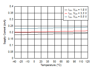
GUID-CE152DAD-A56A-450B-B809-8DD625FFC601-low.gif
Reference = VDD, DAC at midscale
Figure 7-30 Supply Current vs Temperature
GUID-20200915-CA0I-MMCG-S3S4-FFPVQTFPBG71-low.svg
DAC at midscale
Figure 7-32 Supply Current vs Supply Voltage
GUID-FE9E0B11-BCC6-48D6-AA22-0CD8E15CE633-low.gif
 
Figure 7-34 Source and Sink Capability
GUID-20200914-CA0I-8GPR-FCBP-TQZQRNWJN4T1-low.svg
Reference = VDD = 5.5 V, DAC code transition from midscale to midscale – 1 LSB, DAC load = 5kΩ || 200pF
Figure 7-36 Glitch Impulse, Falling Edge,
1-LSB Step
GUID-20200914-CA0I-8M5W-MMPL-PB02LZGBDXTN-low.svg
Reference = VDD = 5.5 V, DAC load = 5kΩ || 200pF
Figure 7-38 Full-Scale Settling Time, Falling Edge
GUID-DC4BAEE6-2795-489A-8BAE-664149ECF8C8-low.gif
Reference = VDD = 5.5 V
Figure 7-40 Power-off Glitch
GUID-40039E2E-EABB-45D0-86BE-1E294DFA7D2C-low.gif
Internal reference (gain = 4x), VDD = 5.25 V + 0.25 VPP, DAC at midscale, DAC load = 5kΩ || 200pF
Figure 7-42 DAC Output AC PSRR vs Frequency
GUID-20200831-CA0I-6HTM-2VW6-L8GS7KWZR27K-low.svg
Internal reference (gain = 4x), VDD = 5.5 V
Figure 7-44 DAC Output Noise Spectral Density
GUID-20200914-CA0I-M0RS-X9P5-QNXC58GL0PP2-low.svg
Internal reference (gain = 4x), VDD = 5.5 V, DAC at midscale
Figure 7-46 DAC Output Noise: 0.1 Hz to 10 Hz