SLASEQ4A October   2018  – December 2018 DAC43608 , DAC53608

PRODUCTION DATA.  

  1. Features
  2. Applications
  3. Description
    1.     Device Images
      1.      Simplified Block Diagram
      2.      Programmable Window Comparator
  4. Revision History
  5. Device Comparison Table
  6. Pin Configurations and Functions
    1.     Pin Functions
  7. Specifications
    1. 7.1  Absolute Maximum Ratings
    2. 7.2  ESD Ratings
    3. 7.3  Recommended Operating Conditions
    4. 7.4  Thermal Information
    5. 7.5  Electrical Characteristics
    6. 7.6  Timing Requirements: I2CTM Standard Mode
    7. 7.7  Timing Requirements: I2CTM Fast Mode
    8. 7.8  Timing Requirements: I2CTM Fast+ Mode
    9. 7.9  Timing Requirements: Logic
    10. 7.10 Typical Characteristics: 1.8 V
    11. 7.11 Typical Characteristics: 5.5 V
    12. 7.12 Typical Characteristics
    13. 7.13 Typical Characteristics
  8. Detailed Description
    1. 8.1 Overview
    2. 8.2 Functional Block Diagram
    3. 8.3 Feature Description
      1. 8.3.1 Digital-to-Analog Converter (DAC) Architecture
        1. 8.3.1.1 DAC Transfer Function
        2. 8.3.1.2 DAC Register Update and LDAC Functionality
        3. 8.3.1.3 CLR Functionality
        4. 8.3.1.4 Output Amplifier
      2. 8.3.2 Reference
      3. 8.3.3 Power-on-Reset (POR)
      4. 8.3.4 Software Reset
    4. 8.4 Device Functional Modes
      1. 8.4.1 Power-Down Mode
    5. 8.5 Programming
      1. 8.5.1 F/S Mode Protocol
      2. 8.5.2 DACx3608 I2CTM Update Sequence
      3. 8.5.3 DACx3608 Address Byte
      4. 8.5.4 DACx3608 Command Byte
      5. 8.5.5 DACx3608 Data Byte (MSDB and LSDB)
      6. 8.5.6 DACx3608 I2CTM Read Sequence
    6. 8.6 Register Map
      1. 8.6.1 DEVICE_CONFIG Register (offset = 01h) [reset = 00FFh]
        1. Table 10. DEVICE_CONFIG Register Field Descriptions
      2. 8.6.2 STATUS/TRIGGER Register (offset = 02h) [reset = 0300h for DAC53608, reset = 0500h for DAC43608]
        1. Table 11. STATUS/TRIGGER Register Field Descriptions
      3. 8.6.3 BRDCAST Register (offset = 03h) [reset = 0000h]
        1. Table 12. BRDCAST Register Field Descriptions
      4. 8.6.4 DACn_DATA Register (offset = 08h to 0Fh) [reset = 0000h]
        1. Table 13. DACn_DATA Register Field Descriptions
  9. Application and Implementation
    1. 9.1 Application Information
    2. 9.2 Typical Applications
      1. 9.2.1 Programmable LED Biasing
        1. 9.2.1.1 Design Requirements
        2. 9.2.1.2 Detailed Design Procedure
        3. 9.2.1.3 Application Curve
      2. 9.2.2 Programmable Window Comparator
        1. 9.2.2.1 Design Requirements
        2. 9.2.2.2 Detailed Design Procedure
        3. 9.2.2.3 Application Curve
  10. 10Power Supply Recommendations
  11. 11Layout
    1. 11.1 Layout Guidelines
    2. 11.2 Layout Example
  12. 12Device and Documentation Support
    1. 12.1 Documentation Support
      1. 12.1.1 Related Documentation
    2. 12.2 Related Links
    3. 12.3 Receiving Notification of Documentation Updates
    4. 12.4 Community Resources
    5. 12.5 Trademarks
    6. 12.6 Electrostatic Discharge Caution
    7. 12.7 Glossary
  13. 13Mechanical, Packaging, and Orderable Information

Package Options

Mechanical Data (Package|Pins)
Thermal pad, mechanical data (Package|Pins)
Orderable Information

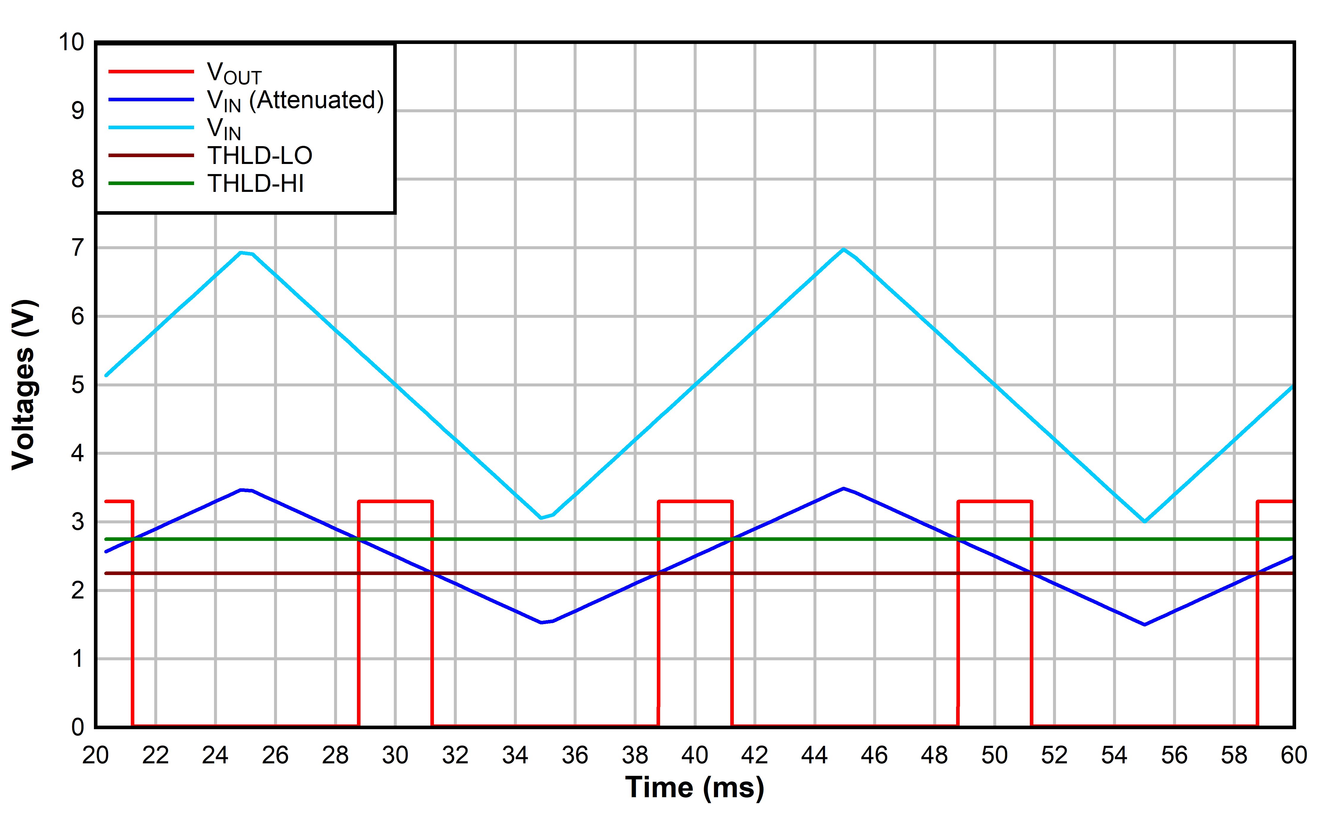
Application Curve

DAC53608 DAC43608 dac53608-programmable-comparator-output-waveform.gif
Figure 67. Programmable Comparator Output Waveform