SLAS452E October 2020 – January 2021 DAC5652
PRODUCTION DATA
- 1 Features
- 2 Applications
- 3 Description
- 4 Revision History
- 5 Pin Configuration and Functions
-
6 Specifications
- 6.1 Absolute Maximum Rationgs
- 6.2 ESD Ratings
- 6.3 Recommended Operating Conditions
- 6.4 Thermal Resistance Characteristics
- 6.5 Electrical Characteristics
- 6.6 Electrical Characteristics
- 6.7 Electrical Characteristics, AC
- 6.8 Electrical Characteristics, DC
- 6.9 Switching Characteristics
- 6.10 Typical Characteristics
- 7 Parameter Measurement Information
- 8 Detailed Description
- 9 Application Information Disclaimer
- 10Power Supply Recommendations
- 11Layout
- 12Device and Documentation Support
- 13Mechanical, Packaging, and Orderable Information
Package Options
Mechanical Data (Package|Pins)
- PFB|48
Thermal pad, mechanical data (Package|Pins)
Orderable Information
7.1.1 Digital Inputs
The data input ports of the DAC5652 accept a standard positive coding with data bits DA9 and DB9 being the most significant bits (MSB). The converter outputs support a clock rate of up to 275 MSPS. The best performance is typically achieved with a symmetric duty cycle for write and clock; however, the duty cycle may vary as long as the timing specifications are met. Similarly, the setup and hold times may be chosen within their specified limits.
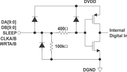
All digital inputs of the DAC5652 are CMOS compatible. Figure 7-1 and Figure 7-2 show schematics of the equivalent CMOS digital inputs of the DAC5652. The pullup and pulldown circuitry is approximately equivalent to 100kΩ.The 10-bit digital data input follows the offset positive binary coding scheme. The DAC5652 is designed to operate with a digital supply (DVDD) of 3 V to 3.6 V.
 Figure 7-1 CMOS/TTL Digital Equivalent Input With Internal Pulldown Resistor
 Figure 7-2 CMOS/TTL Digital Equivalent Input With Internal Pullup Resistor