SLAS452E October 2020 – January 2021 DAC5652
PRODUCTION DATA
- 1 Features
- 2 Applications
- 3 Description
- 4 Revision History
- 5 Pin Configuration and Functions
-
6 Specifications
- 6.1 Absolute Maximum Rationgs
- 6.2 ESD Ratings
- 6.3 Recommended Operating Conditions
- 6.4 Thermal Resistance Characteristics
- 6.5 Electrical Characteristics
- 6.6 Electrical Characteristics
- 6.7 Electrical Characteristics, AC
- 6.8 Electrical Characteristics, DC
- 6.9 Switching Characteristics
- 6.10 Typical Characteristics
- 7 Parameter Measurement Information
- 8 Detailed Description
- 9 Application Information Disclaimer
- 10Power Supply Recommendations
- 11Layout
- 12Device and Documentation Support
- 13Mechanical, Packaging, and Orderable Information
Package Options
Mechanical Data (Package|Pins)
- PFB|48
Thermal pad, mechanical data (Package|Pins)
Orderable Information
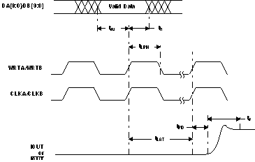
7.1.3 Dual-Bus Data Interface and Timing
In dual-bus mode, the MODE pin is connected to DVDD. The two converter channels within the DAC5652 consist of two independent, 10-bit, parallel data ports. Each DAC channel is controlled by its own set of write (WRTA, WRTB) and clock (CLKA, CLKB) lines. The WRTA/B lines control the channel input latches and the CLKA/B lines control the DAC latches. The data is first loaded into the input latch by a rising edge of the WRTA/B line.
The internal data transfer requires a correct sequence of write and clock inputs, since essentially two clock domains having equal periods (but possibly different phases) are input to the DAC5652. This is defined by a minimum requirement of the time between the rising edge of the clock and the rising edge of the write inputs. This essentially implies that the rising edge of CLKA/B must occur at the same time or before the rising edge of the WRTA/B signal. A minimum delay of 2 ns must be maintained if the rising edge of the clock occurs after the rising edge of the write. Note that these conditions are satisfied when the clock and write inputs are connected externally. Note that all specifications were measured with the WRTA/B and CLKA/B lines connected together.
 Figure 7-3 Dual-Bus Mode Operation