-
DAC5662 Dual, 12-BIT 275 MSPS Digital-to-Analog Converter
- 1 Features
- 2 Applications
- 3 Description
- 4 Revision History
- 5 Pin Configurations and Functions
-
6 Specifications
- 6.1 Absolute Maximum Ratings
- 6.2 ESD Ratings
- 6.3 Recommended Operating Conditions
- 6.4 Thermal Resistance Characteristics
- 6.5 Electrical Characteristics
- 6.6 Electrical Characteristics
- 6.7 Electrical Characteristics, AC
- 6.8 Electrical Characteristics, DC
- 6.9 Switching Characteristics
- 6.10 Typical Characteristics
- 7 Parameter Measurement Information
- 8 Detailed Description
- 9 Application and Implementation
- 10Power Supply Recommendations
- 11Layout
- 12Device and Documentation Support
- IMPORTANT NOTICE
Package Options
Refer to the PDF data sheet for device specific package drawings
Mechanical Data (Package|Pins)
- PFB|48
Thermal pad, mechanical data (Package|Pins)
Orderable Information
DAC5662 Dual, 12-BIT 275 MSPS Digital-to-Analog Converter
1 Features
- 12-Bit dual transmit DAC
- 275 MSPS Update rate
- Single supply: 3 V to 3.6 V
- High SFDR: 85 dBc at 5 MHz
- High IMD3: 78 dBc at 15.1 and 16.1 MHz
- WCDMA ACLR: 70 dB at 30.72 MHz
- Independent or single resistor gain control
- Dual or interleaved data
- On-chip 1.2-V reference
- Low power: 330 mW
- Power-down mode: 15 mW
- Package: 48-Pin TQFP
2 Applications
- Cellular base transceiver station
transmit channel
- CDMA: W-CDMA, CDMA2000, IS-95
- TDMA: GSM, IS-136, EDGE/UWC-136
- Medical, test instrumentation
- Arbitrary waveform generators (AWG)
- Direct digital synthesis (DDS)
- Cable modem termination system (CMTS)
3 Description
The DAC5662 is a monolithic, dual-channel 12-bit high-speed digital-to-analog converter (DAC) with on-chip voltage reference.
Operating with update rates of up to 275 MSPS, the DAC5662 offers exceptional dynamic performance and tight-gain and offset matching, characteristics that make it suitable in either I/Q baseband or direct IF communication applications.
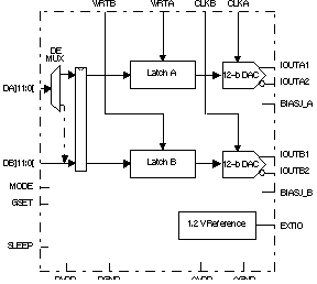
Each DAC has a high-impedance differential current output, suitable for single-ended or differential analog-output configurations. External resistors allow scaling the full-scale output current for each DAC separately or together, typically between 2 mA and 20 mA. An accurate on-chip voltage reference is temperature compensated and delivers a stable 1.2-V reference voltage. Optionally, an external reference may be used.
The DAC5662 has two 12-bit parallel input ports with separate clocks and data latches. For flexibility, the DAC5662 also supports multiplexed data for each DAC on one port when operating in the interleaved mode.
The DAC5662 has been specifically
designed for a differential transformer coupled output with a 50-Ω doubly terminated
load. For a 20-mA full-scale output current a 4:1 impedance ratio (resulting in an
output power of
4 dBm) and 1:1 impedance ratio
transformer (-2 dBm output power) are supported.
The DAC5662 is available in a 48-pin thin quad FlatPack (TQFP). Pin compatibility between family members provides 12-bit (DAC5662) and 14-bit (DAC5672) resolution. Furthermore, the DAC5662 is pin compatible to the DAC2902 and AD9765 dual DACs. The device is characterized for operation over the industrial temperature range of -40°C to 85°C.
| PART NUMBER | PACKAGE(1) | BODY SIZE (NOM) |
|---|---|---|
| DAC5662 | TQFP | 7.00 mm x 7.00 mm |
 Functional Block diagram
4 Revision History
Changes from Revision C (October 2020) to Revision D (October 2021)
- Chnaged the device number from: DAC566452 to: DAC5662 in the Device Information tableGo
Changes from Revision B (July 2004) to Revision C (October 2020)
- Added Device Information table, ESD Ratings table, Thermal Resistance Characteristics table, Feature Description section, Device Functional Modes, Application and Implementation section, Power Supply Recommendations section, Layout section, Device and Documentation Support section, and Mechanical, Packaging, and Orderable Information sectionGo
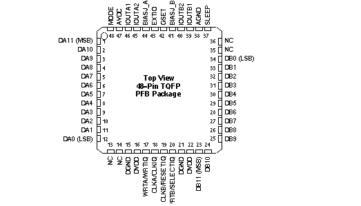
5 Pin Configurations and Functions

| PIN | I/O | DESCRIPTION | |
|---|---|---|---|
| NAME | NO. | ||
| AGND | 38 | I | Analog ground |
| AVDD | 47 | I | Analog supply voltage |
| BIASJ_A | 44 | O | Full-scale output current bias for DACA |
| BIASJ_B | 41 | O | Full-scale output current bias for DACB |
| CLKA/CLKIQ | 18 | I | Clock input for DACA, CLKIQ in interleaved mode. |
| CLKB/RESETIQ | 19 | I | Clock input for DACB, RESETIQ in interleaved mode. |
| DA[11:0] | 1-12 | I | Data port A. DA11 is MSB and DA0 is LSB. Internal pulldown. |
| DB[11:0] | 23-34 | I | Data port B. DB11 is MSB and DB0 is LSB. Internal pulldown. |
| DGND | 15, 21 | I | Digital ground |
| DVDD | 16, 22 | I | Digital supply voltage |
| EXTIO | 43 | I/O | Internal reference output (bypass with 0.1 μF to AGND) or external reference input. |
| GSET | 42 | I | Gain-setting mode: H - 1 resistor, L - 2 resistors. Internal pullup. |
| IOUTA1 | 46 | O | DACA current output. Full-scale with all bits of DA high. |
| IOUTA2 | 45 | O | DACA complementary current output. Full-scale with all bits of DA low. |
| IOUTB1 | 39 | O | DACB current output. Full-scale with all bits of DB high. |
| IOUTB2 | 40 | O | DACB complementary current output. Full-scale with all bits of DB low. |
| MODE | 48 | I | Mode Select: H – Dual Bus, L – Interleaved. Internal pullup. |
| NC | 13, 14, 35, 36 | - | No connection |
| SLEEP | 37 | I | Sleep function control input: H – DAC in power-down mode, L – DAC in operating mode. Internal pulldown. |
| WRTA/WRTIQ | 17 | I | Input write signal for PORT A (WRTIQ in interleaving mode). |
| WRTB/SELECTIQ | 20 | I | Input write signal for PORT B (SELECTIQ in interleaving mode). |