SBAS334D November 2004 – July 2016 DAC5675A
PRODUCTION DATA.
- 1 Features
- 2 Applications
- 3 Description
- 4 Revision History
- 5 Description Continued
- 6 Pin Configuration and Functions
- 7 Specifications
- 8 Detailed Description
- 9 Application and Implementation
- 10Power Supply Recommendations
- 11Layout
- 12Device and Documentation Support
- 13Mechanical, Packaging, and Orderable Information
Package Options
Mechanical Data (Package|Pins)
- PHP|48
Thermal pad, mechanical data (Package|Pins)
- PHP|48
Orderable Information
8 Detailed Description
8.1 Overview
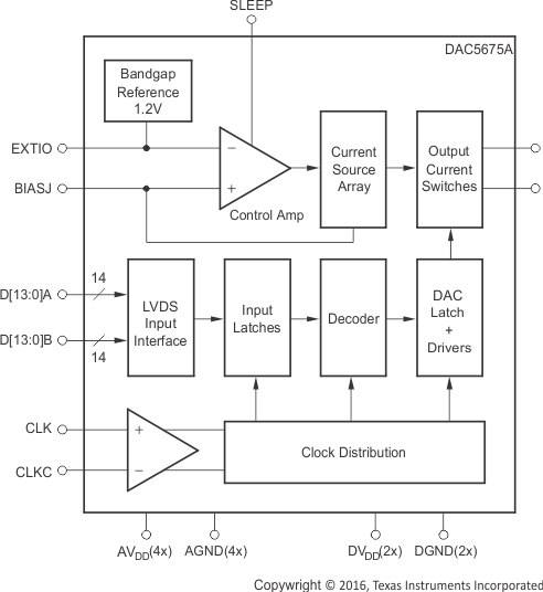
The DAC5675A is a 14-bit resolution high-speed digital-to-analog converter. The DAC5675A is designed or high-speed digital data transmission in wired and wireless communication systems, high frequency direct-digital synthesis (DDS), and waveform reconstruction in test and measurement applications. The DAC5675A has excellent spurious free dynamic range (SFDR) at high intermediate frequencies, which makes the DAC5675A well-suited for multicarrier transmission in TDMA- and CDMA based cellular base transceiver stations (BTSs).
8.2 Functional Block Diagram
8.3 Feature Description
8.3.1 Digital Inputs
The DAC5675A uses a low voltage differential signaling (LVDS) bus input interface. The LVDS features a low differential voltage swing with low constant power consumption (≉4mA per complementary data input) across frequency. The differential characteristic of LVDS allows for high-speed data transmission with low electromagnetic interference (EMI) levels. The LVDS input minimum and maximum input threshold table lists the LVDS input levels. Figure 13 shows the equivalent complementary digital input interface for the DAC5675A, valid for pins D[13:0]A and D[13:0]B. Note that the LVDS interface features internal 110Ω resistors for proper termination. Figure 2 shows the LVDS input timing measurement circuit and waveforms. A common-mode level of 1.2V and a differential input swing of 0.8VPP is applied to the inputs.
Figure 14 shows a schematic of the equivalent CMOS/TTL-compatible digital inputs of the DAC5675A, valid for the SLEEP pin.
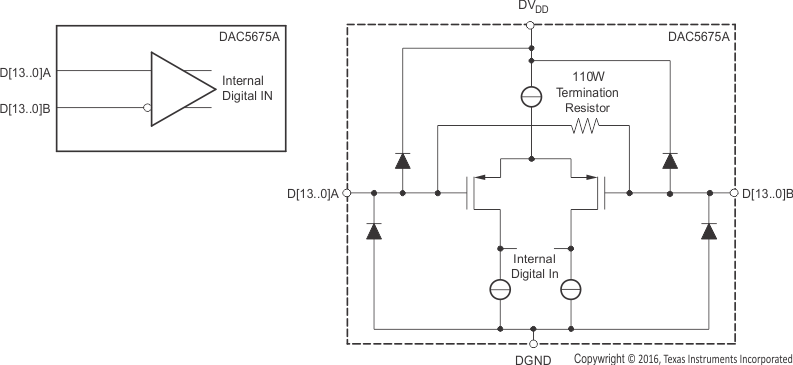 Figure 13. LVDS Digital Equivalent Input
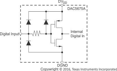 Figure 14. CMOS/TTL Digital Equivalent Input
8.3.2 Clock Input
The DAC5675A features differential, LVPECL compatible clock inputs (CLK, CLKC). Figure 15 shows the equivalent schematic of the clock input buffer. The internal biasing resistors set the input common-mode voltage to approximately 2V, while the input resistance is typically 670Ω. A variety of clock sources can be ac-coupled to the device, including a sine wave source (see Figure 16).
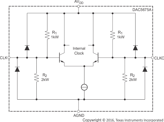 Figure 15. Clock Equivalent Input
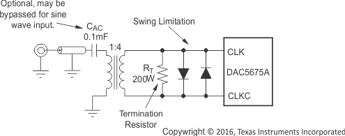 Figure 16. Driving the DAC5675A with a Single-Ended Clock Source Using a Transformer
To obtain best ac performance the DAC5675A clock input should be driven with a differential LVPECL or sine wave source as shown in Figure 17 and Figure 18. Here, the potential of VTT should be set to the termination voltage required by the driver along with the proper termination resistors (RT). The DAC5675A clock input can also be driven single-ended; this is shown in Figure 19.
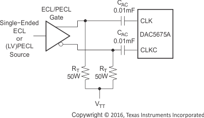 Figure 17. Driving the DAC5675A with a Single-Ended ECL/PECL Clock Source
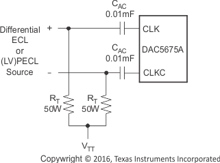 Figure 18. Driving the DAC5675A with a Differential ECL/PECL Clock Source
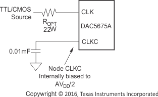 Figure 19. Driving the DAC5675A with a Single-Ended TTL/CMOS Clock Source
8.3.3 Supply Inputs
The DAC5675A comprises separate analog and digital supplies, that is, AVDD and DVDD, respectively. These supply inputs can be set independently from 3.6V down to 3.15V.
8.3.4 DAC Transfer Function
The DAC5675A has a current sink output. The current flow through IOUT1 and IOUT2 is controlled by D[13:0]A and D[13:0]B. For ease of use, we denote D[13:0] as the logical bit equivalent of D[13:0]A and its complement D[13:0]B. The DAC5675A supports straight binary coding with D13 being the MSB and D0 the LSB. Full-scale current flows through IOUT2 when all D[13:0] inputs are set high and through IOUT1 when all D[13:0] inputs are set low. The relationship between IOUT1 and IOUT2 can be expressed asEquation 1:

IO(FS) is the full-scale output current sink (2mA to 20mA). Since the output stage is a current sink, the current can only flow from AVDD through the load resistors RL into the IOUT1 and IOUT2 pins.
The output current flow in each pin driving a resistive load can be expressed as shown in Figure 20, as well as in Equation 2 and Equation 3.
![DAC5675A Relationship Between
D[13:0], IOUT1 and IOUT2 DAC5675A dac-xfer_bas334.gif](/ods/images/SBAS334D/dac-xfer_bas334.gif) Figure 20. Relationship Between D[13:0], IOUT1 and IOUT2
Figure 20. Relationship Between D[13:0], IOUT1 and IOUT2


where CODE is the decimal representation of the DAC input word. This would translate into single-ended voltages at IOUT1 and IOUT2, as shown in Equation 4 and Equation 5:


Assuming that D[13:0] = 1 and the RL is 50Ω, the differential voltage between pins IOUT1 and IOUT2 can be expressed as shown in Equation 6 through Equation 8:


If D[13:0] = 0, then IOUT2 = 0mA and IOUT1 = 20mA and the differential voltage VDIFF = –1V.
The output currents and voltages in IOUT1 and IOUT2 are complementary. The voltage, when measured differentially, will be doubled compared to measuring each output individually. Care must be taken not to exceed the compliance voltages at the IOUT1 and IOUT2 pins in order to keep signal distortion low.
8.3.5 Reference Operation
The DAC5675A has a bandgap reference and control amplifier for biasing the full-scale output current. The full-scale output current is set by applying an external resistor RBIAS. The bias current IBIAS through resistor RBIAS is defined by the on-chip bandgap reference voltage and control amplifier. The full-scale output current equals 16 times this bias current. The full-scale output current IO(FS) is thus expressed as Equation 9:

where VEXTIO is the voltage at terminal EXTIO. The bandgap reference voltage delivers a stable voltage of 1.2 V. This reference can be overridden by applying an external voltage to terminal EXTIO. The bandgap reference can additionally be used for external reference operation. In such a case, an external buffer amplifier with high impedance input should be selected in order to limit the bandgap load current to less than 100 nA. The capacitor CEXT may be omitted. Terminal EXTIO serves as either an input or output node. The full-scale output current is adjustable from 20mA down to 2mA by varying resistor RBIAS.
8.3.6 Analog Current Outputs
Figure 21 shows a simplified schematic of the current sink array output with corresponding switches. Differential NPN switches direct the current of each individual NPN current sink to either the positive output node IOUT1 or its complementary negative output node IOUT2. D[13:0] controls the S(N)C current switches and D[13:0] controls the S(N) current switches, as explained in the previous DAC Transfer Function section (see Figure 20). The output impedance is determined by the stack of the current sinks and differential switches, and is > 300kΩ in parallel with an output capacitance of 5pF.
The external output resistors are referred to the positive supply AVDD.
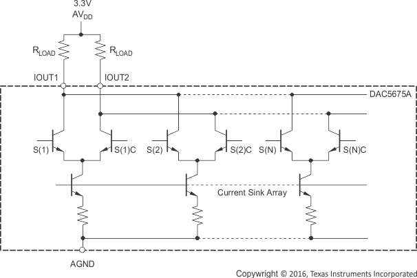 Figure 21. Equivalent Analog Current Output
The DAC5675A can easily be configured to drive a doubly-terminated 50Ω cable using a properly selected transformer. Figure 22 and Figure 23 show the 1:1 and 4:1 impedance ratio configuration, respectively. These configurations provide maximum rejection of common-mode noise sources and even-order distortion components, thereby doubling the power of the DAC to the output. The center tap on the primary side of the transformer is terminated to AVDD, enabling a dc current flow for both IOUT1 and IOUT2. Note that the ac performance of the DAC5675A is optimum and specified using a 1:1 differential transformer-coupled output.
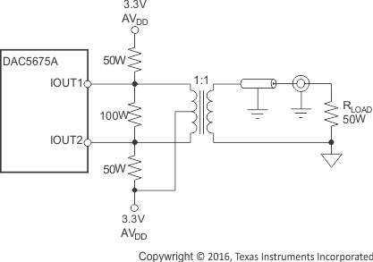 Figure 22. Driving a Doubly-Terminated 50Ω Cable Using a 1:1 Impedance Ratio Transformer
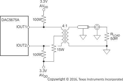 Figure 23. Driving a Doubly-Terminated 50Ω Cable Using a 4:1 Impedance Ratio Transformer
Figure 24(a) shows the typical differential output configuration with two external matched resistor loads. The nominal resistor load of 25 Ω gives a differential output swing of 1VPP (0.5–VPP single-ended) when applying a 20 mA full-scale output current. The output impedance of the DAC5675A slightly depends on the output voltage at nodes IOUT1 and IOUT2. Consequently, for optimum dc-integral nonlinearity, the configuration of Figure 24(b) should be chosen. In this current/voltage (I-V) configuration, terminal IOUT1 is kept at AVDD by the inverting operational amplifier. The complementary output should be connected to AVDD to provide a dc-current path for the current sources switched to IOUT1. The amplifier maximum output swing and the full-scale output current of the DAC determine the value of the feedback resistor (RFB). The capacitor (CFB) filters the steep edges of the DAC5675A current output, thereby reducing the operational amplifier slew-rate requirements. In this configuration, the op amp should operate at a supply voltage higher than the resistor output reference voltage AVDD as a result of its positive and negative output swing around AVDD. Node IOUT1 should be selected if a single-ended unipolar output is desired.
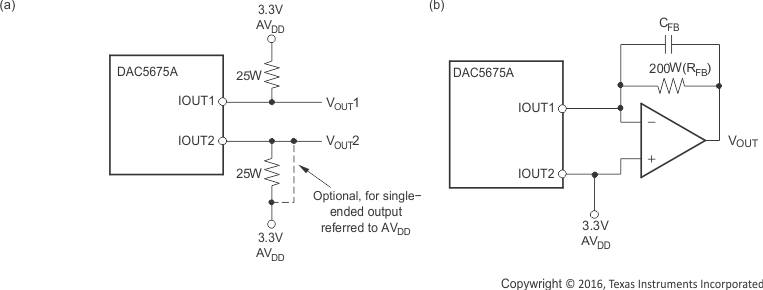 Figure 24. Output Configurations
8.4 Device Functional Modes
8.4.1 Sleep Mode
The DAC5675A features a power-down mode that turns off the output current and reduces the supply current to approximately 6mA. The power-down mode is activated by applying a logic level 1 to the SLEEP pin pulled down internally.