SBAS793A November   2019  – April 2020 DAC60502 , DAC70502 , DAC80502

PRODUCTION DATA.  

  1. Features
  2. Applications
  3. Description
    1.     Device Images
      1.      Functional Block Diagram
  4. Revision History
  5. Device Comparison Table
  6. Pin Configuration and Functions
    1.     Pin Functions
  7. Specifications
    1. 7.1  Absolute Maximum Ratings
    2. 7.2  ESD Ratings
    3. 7.3  Recommended Operating Conditions
    4. 7.4  Thermal Information
    5. 7.5  Electrical Characteristics
    6. 7.6  Timing Requirements : SPI Mode
    7. 7.7  Timing Requirements : I2C Standard Mode
    8. 7.8  Timing Requirements : I2C Fast Mode
    9. 7.9  Timing Requirements : I2C Fast-Mode Plus
    10. 7.10 Typical Characteristics
  8. Detailed Description
    1. 8.1 Overview
    2. 8.2 Functional Block Diagram
    3. 8.3 Feature Description
      1. 8.3.1 Digital-to-Analog Converter (DAC) Architecture
        1. 8.3.1.1 DAC Transfer Function
        2. 8.3.1.2 DAC Register Structure
        3. 8.3.1.3 Output Amplifier
      2. 8.3.2 Internal Reference
        1. 8.3.2.1 Solder Heat Reflow
      3. 8.3.3 Power-On Reset (POR)
      4. 8.3.4 Software Reset
    4. 8.4 Device Functional Modes
      1. 8.4.1 Power-Down Mode
    5. 8.5 Programming
      1. 8.5.1 Serial Interface
        1. 8.5.1.1 SPI Mode
          1. 8.5.1.1.1 SYNC Interrupt
        2. 8.5.1.2 I2C Mode
          1. 8.5.1.2.1 F/S Mode Protocol
          2. 8.5.1.2.2 DACx0502 I2C Update Sequence
            1. 8.5.1.2.2.1 DACx0502 Address Byte
            2. 8.5.1.2.2.2 DACx0502 Command Byte
            3. 8.5.1.2.2.3 DACx0502 Data Byte (MSDB and LSDB)
          3. 8.5.1.2.3 DACx0502 I2C Read Sequence
    6. 8.6 Register Maps
      1. 8.6.1 Registers
        1. 8.6.1.1 NOOP Register (offset = 0h) [reset = 0000h]
          1. Table 9. NOOP Register Field Descriptions
        2. 8.6.1.2 DEVID Register (offset = 1h) [reset = 0214h for DAC80502, 1214h for DAC70502, 2214h for DAC60502]
          1. Table 10. DEVID Register Field Descriptions
        3. 8.6.1.3 SYNC Register (offset = 2h) [reset = 0300h]
          1. Table 11. SYNC Register Field Descriptions
        4. 8.6.1.4 CONFIG Register (offset = 3h) [reset = 0000h]
          1. Table 12. CONFIG Register Field Descriptions
        5. 8.6.1.5 GAIN Register (offset = 4h) [reset = 0003h]
          1. Table 13. GAIN Register Field Descriptions
        6. 8.6.1.6 TRIGGER Register (offset = 5h) [reset = 0000h]
          1. Table 14. TRIGGER Register Field Descriptions
        7. 8.6.1.7 BRDCAST Register (offset = 6h) [reset = 0000h for RSTSEL = 0, or reset = 8000h for RSTSEL = 1]
          1. Table 15. BRDCAST Register Field Descriptions
        8. 8.6.1.8 STATUS Register (offset = 7h) [reset = 0000h]
          1. Table 16. STATUS Register Field Descriptions
        9. 8.6.1.9 DAC-n Register (offset = 8h–9h) [reset = 0000h for RSTSEL = 0, or reset = 8000h for RSTSEL = 1]
          1. Table 17. DAC-A Data Register Field Descriptions (8h)
          2. Table 18. DAC-B Data Register Field Descriptions (9h)
  9. Application and Implementation
    1. 9.1 Application Information
    2. 9.2 Typical Application
      1. 9.2.1 Design Requirements
      2. 9.2.2 Detailed Design Procedure
      3. 9.2.3 Application Curves
    3. 9.3 System Examples
      1. 9.3.1 SPI Connection to a Processor
      2. 9.3.2 I2C Interface Connection to a Processor
    4. 9.4 What To Do and What Not To Do
      1. 9.4.1 What To Do
      2. 9.4.2 What Not To Do
    5. 9.5 Initialization Setup
  10. 10Power Supply Recommendations
  11. 11Layout
    1. 11.1 Layout Guidelines
    2. 11.2 Layout Example
  12. 12Device and Documentation Support
    1. 12.1 Documentation Support
      1. 12.1.1 Related Documentation
    2. 12.2 Related Links
    3. 12.3 Receiving Notification of Documentation Updates
    4. 12.4 Support Resources
    5. 12.5 Trademarks
    6. 12.6 Electrostatic Discharge Caution
    7. 12.7 Glossary
  13. 13Mechanical, Packaging, and Orderable Information

Package Options

Mechanical Data (Package|Pins)
Thermal pad, mechanical data (Package|Pins)
Orderable Information

Typical Characteristics

at TA = 25°C, VDD = 5.5 V, internal reference = 2.5 V, REF-DIV = 0 and BUFF-GAIN = 1, channel A shown, and DAC outputs unloaded (unless otherwise noted)
DAC80502 DAC70502 DAC60502 D001.gif
Figure 3. Integral Linearity Error vs Digital Input Code
DAC80502 DAC70502 DAC60502 D003.gif
Figure 5. Total Unadjusted Error vs Digital Input Code
DAC80502 DAC70502 DAC60502 D005.gif
Figure 7. Differential Linearity Error vs Temperature
DAC80502 DAC70502 DAC60502 D007.gif
Figure 9. Zero-Code Error vs Temperature
DAC80502 DAC70502 DAC60502 D009.gif
Figure 11. Full-Scale Error vs Temperature
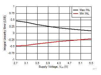
DAC80502 DAC70502 DAC60502 D011.gif
REF-DIV = 0 and BUFF-GAIN = 0
Figure 13. Integral Linearity Error vs Supply Voltage
DAC80502 DAC70502 DAC60502 D013.gif
Figure 15. Total Unadjusted Error vs Supply Voltage
DAC80502 DAC70502 DAC60502 D015.gif
Figure 17. Offset Error vs Supply Voltage
DAC80502 DAC70502 DAC60502 D017.gif
Figure 19. Full-Scale Error vs Supply Voltage
DAC80502 DAC70502 DAC60502 D019.gif
Figure 21. Differential Linearity Error vs Reference Voltage
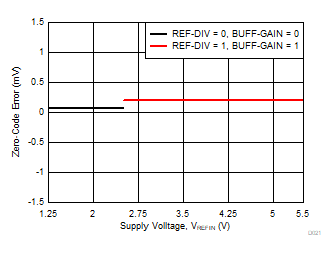
DAC80502 DAC70502 DAC60502 D021.gif
Figure 23. Zero-Code Error vs Reference Voltage
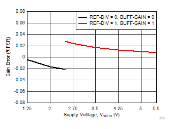
DAC80502 DAC70502 DAC60502 D023.gif
Figure 25. Gain Error vs Reference Voltage
DAC80502 DAC70502 DAC60502 D025.gif
Figure 27. Supply Current vs Digital Input Code
DAC80502 DAC70502 DAC60502 D027.gif
DAC code at midscale
Figure 29. Supply Current vs Supply Voltage
DAC80502 DAC70502 DAC60502 D029.gif
External reference = 2.5 V, REF-DIV = 1 and BUFF-GAIN = 0
Figure 31. Power Down Current vs Supply Voltage
DAC80502 DAC70502 DAC60502 D031.gif
REF-DIV = 0 and BUFF-GAIN = 0
Figure 33. Source and Sink Capability
DAC80502 DAC70502 DAC60502 D033.gif
REF-DIV = 1 and BUFF-GAIN = 0
Figure 35. Source and Sink Capability
DAC80502 DAC70502 DAC60502 D035.gif
DAC code transition from midscale to midscale – 1 LSB,
REF-DIV = 0 and BUFF-GAIN = 0
Figure 37. Glitch Impulse, Falling Edge, 1-LSB Step
DAC80502 DAC70502 DAC60502 D037.gif
REF-DIV = 0 and BUFF-GAIN = 0
Figure 39. Full-Scale Settling Time, Falling Edge
DAC80502 DAC70502 DAC60502 D039.gif
REF-DIV = 0 and BUFF-GAIN = 0
Figure 41. Power-Off Glitch
DAC80502 DAC70502 DAC60502 D041.gif
fo = 1 kHz, fs = 400 kHz, includes 7 harmonics,
measurement bandwidth = 20 kHz, external reference = 2.5 V,
REF-DIV = 0 and BUFF-GAIN = 0
Figure 43. DAC Output THD+N vs Frequency
DAC80502 DAC70502 DAC60502 D043.gif
DAC code at midscale, external reference = 2.5 V,
REF-DIV = 0 and BUFF-GAIN = 0
Figure 45. DAC Output Noise: 0.1 Hz to 10 Hz
DAC80502 DAC70502 DAC60502 D045.gif
SCLK = 1 MHz, DAC code at midscale, external reference = 2.5 V,
REF-DIV = 0 and BUFF-GAIN = 0
Figure 47. Clock Feedthrough
DAC80502 DAC70502 DAC60502 D047.gif
Figure 49. Internal Reference Voltage vs Supply Voltage
DAC80502 DAC70502 DAC60502 D049.gif
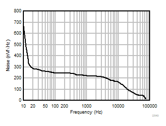
Figure 51. Internal Reference Noise Density vs Frequency
DAC80502 DAC70502 DAC60502 D051.gif
Figure 53. Internal Reference Temperature Drift Histogram
DAC80502 DAC70502 DAC60502 D054.gif
Figure 55. Internal Reference Temperature Drift (Pre-Solder and Post-Solder) Histogram
DAC80502 DAC70502 DAC60502 D002.gif
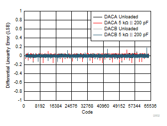
Figure 4. Differential Linearity Error vs Digital Input Code
DAC80502 DAC70502 DAC60502 D004.gif
Figure 6. Integral Linearity Error vs Temperature
DAC80502 DAC70502 DAC60502 D006.gif
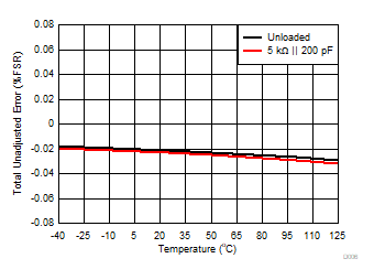
Figure 8. Total Unadjusted Error vs Temperature
DAC80502 DAC70502 DAC60502 D008.gif
Figure 10. Offset Error vs Temperature
DAC80502 DAC70502 DAC60502 D010.gif
Figure 12. Gain Error vs Temperature
DAC80502 DAC70502 DAC60502 D012.gif
REF-DIV = 0 and BUFF-GAIN = 0
Figure 14. Differential Linearity Error vs Supply Voltage
DAC80502 DAC70502 DAC60502 D014.gif
Figure 16. Zero-Code Error vs Supply Voltage
DAC80502 DAC70502 DAC60502 D016.gif
Figure 18. Gain Error vs Supply Voltage
DAC80502 DAC70502 DAC60502 D018.gif
Figure 20. Integral Linearity Error vs Reference Voltage
DAC80502 DAC70502 DAC60502 D020.gif
Figure 22. Total Unadjusted Error vs Reference Voltage
DAC80502 DAC70502 DAC60502 D022.gif
Figure 24. Offset Error vs Reference Voltage
DAC80502 DAC70502 DAC60502 D024.gif
Figure 26. Full-Scale Error vs Reference Voltage
DAC80502 DAC70502 DAC60502 D026.gif
DAC code at midscale
Figure 28. Supply Current vs Temperature
DAC80502 DAC70502 DAC60502 D028.gif
REF-DIV = 0 and BUFF-GAIN = 0
Figure 30. Power-Down Current vs Temperature
DAC80502 DAC70502 DAC60502 D030.gif
External reference = 2.5 V
Figure 32. Headroom and Footroom vs Load Current
DAC80502 DAC70502 DAC60502 D032.gif
REF-DIV = 0 and BUFF-GAIN = 1
Figure 34. Source and Sink Capability
DAC80502 DAC70502 DAC60502 D034.gif
DAC code transition from midscale – 1 to midscale LSB,
REF-DIV = 0 and BUFF-GAIN = 0
Figure 36. Glitch Impulse, Rising Edge, 1-LSB Step
DAC80502 DAC70502 DAC60502 D036.gif
REF-DIV = 0 and BUFF-GAIN = 0
Figure 38. Full-Scale Settling Time, Rising Edge
DAC80502 DAC70502 DAC60502 D038.gif
REF-DIV = 0 and BUFF-GAIN = 0
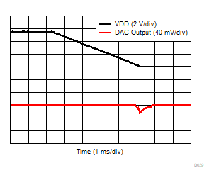
Figure 40. Power-On Glitch
DAC80502 DAC70502 DAC60502 D040.gif
DAC code at midscale, VDD = 5.0 V + 0.2 VPP,
REF-DIV = 0 and BUFF-GAIN = 0
Figure 42. DAC Output AC PSRR vs Frequency
DAC80502 DAC70502 DAC60502 D042.gif
Gain = 1X (REF-DIV = 1 and BUFF-GAIN = 1),
external reference = 2.5 V,
REF-DIV = 0 and BUFF-GAIN = 0
Figure 44. DAC Output Noise Spectral Density
DAC80502 DAC70502 DAC60502 D044.gif
DAC code at midscale, internal reference = 2.5 V,
REF-DIV = 0 and BUFF-GAIN = 0
Figure 46. DAC Output Noise: 0.1 Hz to 10 Hz
DAC80502 DAC70502 DAC60502 D046.gif
30 units
Figure 48. Internal Reference Voltage vs Temperature
DAC80502 DAC70502 DAC60502 D048.gif
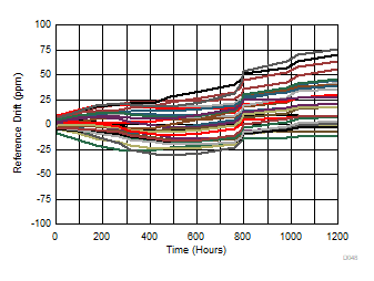
Figure 50. Internal Reference Voltage vs Time
DAC80502 DAC70502 DAC60502 D050.gif
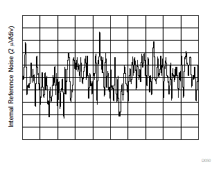
Figure 52. Internal Reference Noise: 0.1 Hz to 10 Hz
DAC80502 DAC70502 DAC60502 D053.gif
Figure 54. Internal Reference Initial Accuracy
(Pre- and Post-Solder) Histogram