SBAS442D august 2008 – august 2023 DAC5311 , DAC6311 , DAC7311
PRODUCTION DATA
- 1
- 1 Features
- 2 Applications
- 3 Description
- 4 Revision History
- 5 Device Comparison
- 6 Pin Configuration and Functions
-
7 Specifications
- 7.1 Absolute Maximum Ratings
- 7.2 ESD Ratings
- 7.3 Recommended Operating Conditions
- 7.4 Thermal Information
- 7.5 Electrical Characteristics
- 7.6 Timing Requirements
- 7.7 Timing Diagrams
- 7.8 Typical Characteristics: AVDD = 5 V
- 7.9 Typical Characteristics: AVDD = 3.6 V
- 7.10 Typical Characteristics: AVDD = 2.7 V
- 8 Detailed Description
- 9 Application and Implementation
- 10Device and Documentation Support
- 11Mechanical, Packaging, and Orderable Information
Package Options
Mechanical Data (Package|Pins)
- DCK|6
Thermal pad, mechanical data (Package|Pins)
Orderable Information
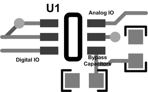
9.4.2 Layout Example
 Figure 9-10 Recommended Layout