SLAS767B June   2011  – March 2015 DAC7551-Q1

PRODUCTION DATA.  

  1. Features
  2. Applications
  3. Description
  4. Revision History
  5. Pin Configuration and Functions
  6. Specifications
    1. 6.1 Absolute Maximum Ratings
    2. 6.2 ESD Ratings
    3. 6.3 Recommended Operating Conditions
    4. 6.4 Thermal Information
    5. 6.5 Electrical Characteristics
    6. 6.6 Timing Requirements
    7. 6.7 Typical Characteristics
  7. Detailed Description
    1. 7.1 Overview
    2. 7.2 Functional Block Diagram
    3. 7.3 Feature Description
      1. 7.3.1 Digital-to-Analog Converter
      2. 7.3.2 Resistor String
      3. 7.3.3 Output Buffer Amplifiers
        1. 7.3.3.1 DAC External Reference Input
        2. 7.3.3.2 Amplifier Sense Input
        3. 7.3.3.3 Power-On Reset
        4. 7.3.3.4 Power Down
        5. 7.3.3.5 Asynchronous Clear
        6. 7.3.3.6 IOVDD and Level Shifters
      4. 7.3.4 Integral and Differential Linearity
      5. 7.3.5 Glitch Energy
    4. 7.4 Device Functional Modes
    5. 7.5 Programming
      1. 7.5.1 Serial Interface
        1. 7.5.1.1 16-Bit Word and Input Shift Register
        2. 7.5.1.2 Daisy-Chain Operation
  8. Application and Implementation
    1. 8.1 Application Information
      1. 8.1.1 Waveform Generation
      2. 8.1.2 Generating ±5-V, ±10-V, and ±12-V Outputs For Precision Industrial Control
        1. 8.1.2.1 Loop Accuracy
        2. 8.1.2.2 Loop Speed
    2. 8.2 Typical Application
      1. 8.2.1 Generating Industrial Voltage Ranges
        1. 8.2.1.1 Design Requirements
        2. 8.2.1.2 Detailed Design Procedure
        3. 8.2.1.3 Application Curves
  9. Power Supply Recommendations
  10. 10Layout
    1. 10.1 Layout Guidelines
    2. 10.2 Layout Example
  11. 11Device and Documentation Support
    1. 11.1 Documentation Support
      1. 11.1.1 Related Documentation
    2. 11.2 Trademarks
    3. 11.3 Electrostatic Discharge Caution
    4. 11.4 Glossary
  12. 12Mechanical, Packaging, and Orderable Information

Package Options

Mechanical Data (Package|Pins)
Thermal pad, mechanical data (Package|Pins)
Orderable Information

10 Layout

10.1 Layout Guidelines

A precision analog component requires careful layout, adequate bypassing, and clean, well-regulated power supplies. The DAC7551-Q1 device offers single-supply operation, and is often used in close proximity with digital logic, microcontrollers, microprocessors, digital signal processors, or a combination. The more digital logic present in the design and the higher the switching speed, the more difficult it is to prevent digital noise from appearing at the output. As a result of the single ground pin of the DAC7551-Q1 device, all return currents (including digital and analog return currents for the DAC) must flow through a single point. Ideally, the GND should be connected directly to an analog ground plane. This plane should be separate from the ground connection for the digital components until these components were connected at the power-entry point of the system.

10.2 Layout Example
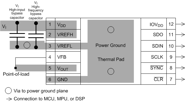
DAC7551-Q1 layout_slas767.gifFigure 32. DAC7551-Q1 Layout Example