SLAS767B June   2011  – March 2015 DAC7551-Q1

PRODUCTION DATA.  

  1. Features
  2. Applications
  3. Description
  4. Revision History
  5. Pin Configuration and Functions
  6. Specifications
    1. 6.1 Absolute Maximum Ratings
    2. 6.2 ESD Ratings
    3. 6.3 Recommended Operating Conditions
    4. 6.4 Thermal Information
    5. 6.5 Electrical Characteristics
    6. 6.6 Timing Requirements
    7. 6.7 Typical Characteristics
  7. Detailed Description
    1. 7.1 Overview
    2. 7.2 Functional Block Diagram
    3. 7.3 Feature Description
      1. 7.3.1 Digital-to-Analog Converter
      2. 7.3.2 Resistor String
      3. 7.3.3 Output Buffer Amplifiers
        1. 7.3.3.1 DAC External Reference Input
        2. 7.3.3.2 Amplifier Sense Input
        3. 7.3.3.3 Power-On Reset
        4. 7.3.3.4 Power Down
        5. 7.3.3.5 Asynchronous Clear
        6. 7.3.3.6 IOVDD and Level Shifters
      4. 7.3.4 Integral and Differential Linearity
      5. 7.3.5 Glitch Energy
    4. 7.4 Device Functional Modes
    5. 7.5 Programming
      1. 7.5.1 Serial Interface
        1. 7.5.1.1 16-Bit Word and Input Shift Register
        2. 7.5.1.2 Daisy-Chain Operation
  8. Application and Implementation
    1. 8.1 Application Information
      1. 8.1.1 Waveform Generation
      2. 8.1.2 Generating ±5-V, ±10-V, and ±12-V Outputs For Precision Industrial Control
        1. 8.1.2.1 Loop Accuracy
        2. 8.1.2.2 Loop Speed
    2. 8.2 Typical Application
      1. 8.2.1 Generating Industrial Voltage Ranges
        1. 8.2.1.1 Design Requirements
        2. 8.2.1.2 Detailed Design Procedure
        3. 8.2.1.3 Application Curves
  9. Power Supply Recommendations
  10. 10Layout
    1. 10.1 Layout Guidelines
    2. 10.2 Layout Example
  11. 11Device and Documentation Support
    1. 11.1 Documentation Support
      1. 11.1.1 Related Documentation
    2. 11.2 Trademarks
    3. 11.3 Electrostatic Discharge Caution
    4. 11.4 Glossary
  12. 12Mechanical, Packaging, and Orderable Information

Package Options

Mechanical Data (Package|Pins)
Thermal pad, mechanical data (Package|Pins)
Orderable Information

5 Pin Configuration and Functions

DRN Package
12-Pin USON With Exposed Thermal Pad
Top View
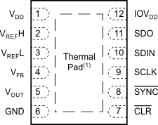
DAC7551-Q1 po_slas767.gif
1. The thermal pad should be connected to GND.

Pin Functions

PIN I/O DESCRIPTION
NO. NAME
1 VDD I Analog voltage supply input
2 VREFH I Positive reference voltage input
3 VREFL I Negative reference voltage input
4 VFB I DAC amplifier sense input.
5 VOUT O Analog output voltage from DAC
6 GND Ground.
7 CLR I Asynchronous input to clear the DAC registers. When the CLR pin is low, the DAC register is set to 000h and the output voltage to 0 V.
8 SYNC I Frame synchronization input. The falling edge of the SYNC pulse indicates the start of a serial data frame shifted out to the DAC7551-Q1 device.
9 SCLK I Serial clock input
10 SDIN I Serial data input
11 SDO O Serial data output
12 IOVDD I I/O voltage supply input