-
DACxx6x-Q1 Automotive Dual 16-, 14-, 12-Bit, Low-Power, Buffered, Voltage-Output DACs With 2.5-V, 4-PPM/°C Internal Reference SLAS950A May 2013 – June 2015 DAC7562-Q1 , DAC7563-Q1 , DAC8162-Q1 , DAC8163-Q1 , DAC8562-Q1 , DAC8563-Q1
PRODUCTION DATA.
-
DACxx6x-Q1 Automotive Dual 16-, 14-, 12-Bit, Low-Power, Buffered, Voltage-Output DACs With 2.5-V, 4-PPM/°C Internal Reference
- 1 Features
- 2 Applications
- 3 Description
- 4 Revision History
- 5 Device Comparison Table
- 6 Pin Configuration and Functions
- 7 Specifications
- 8 Detailed Description
- 9 Application and Implementation
- 10Power Supply Recommendations
- 11Layout
- 12Device and Documentation Support
- 13Mechanical, Packaging, and Orderable Information
- IMPORTANT NOTICE
Package Options
Mechanical Data (Package|Pins)
- DGS|10
Thermal pad, mechanical data (Package|Pins)
Orderable Information
DACxx6x-Q1 Automotive Dual 16-, 14-, 12-Bit, Low-Power, Buffered, Voltage-Output DACs With 2.5-V, 4-PPM/°C Internal Reference
1 Features
- Qualified for Automotive Applications
- AEC-Q100 Qualified with the Following Results:
- Device Temperature Grade 1: –40°C to 125°C Ambient Operating Temperature Range
- Device HBM ESD Classification Level 2
- Device CDM ESD Classification Level C4B
- Relative Accuracy:
- DAC756x (12-Bit): 0.3 LSB INL
- DAC816x (14-Bit): 1 LSB INL
- DAC856x (16-Bit): 4 LSB INL
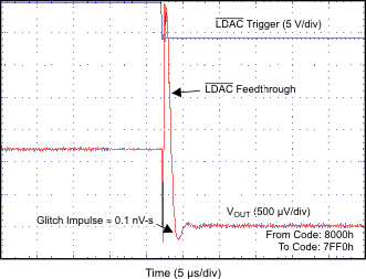
- Glitch Impulse: 0.1 nV-s
- Bidirectional Reference: Input or 2.5-V Output
- Output Disabled by Default
- ±5-mV Initial Accuracy (Max)
- 4-ppm/°C Temperature Drift (Typ)
- 10-ppm/°C Temperature Drift (Max)
- 20-mA Sink and Source Capability
- Power-On Reset to Zero Scale or Mid-Scale
- Low-Power: 4 mW (Typ, 5-V AVDD, Including Internal Reference Current)
- Wide Power-Supply Range: 2.7 V to 5.5 V
- 50-MHz SPI With Schmitt-Triggered Inputs
- LDAC and CLR Functions
- Output Buffer With Rail-to-Rail Operation
- Package: VSSOP-10
2 Applications
- Portable Instrumentation
- PLC Analog Output Module
- Closed-Loop Servo Control
- Voltage Controlled Oscillator Tuning
- Data Acquisition Systems
- Programmable Gain and Offset Adjustment
3 Description
The DAC756x-Q1, DAC816x-Q1, and DAC856x-Q1 (DACxx6x-Q1) devices are low-power, voltage-output, dual-channel, 12-, 14-, and 16-bit digital-to-analog converters (DACs), respectively. These devices include a 2.5-V, 4-ppm/°C internal reference, giving a full-scale output voltage range of 2.5 V or 5 V. The internal reference has an initial accuracy of ±5 mV and can source or sink up to 20 mA at the VREFIN/VREFOUT pin.
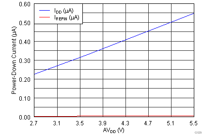
These devices are monotonic, providing excellent linearity and minimizing undesired code-to-code transient voltages (glitch). They use a versatile three-wire serial interface that operates at clock rates up to 50 MHz. The interface is compatible with standard SPI™, QSPI™, Microwire, and digital signal processor (DSP) interfaces. The DACxx62-Q1 devices incorporate a power-on-reset circuit that ensures the DAC output powers up and remains at zero scale until a valid code is written to the device, whereas the DACxx63-Q1 devices similarly power up at mid-scale. These devices contain a power-down feature that reduces current consumption to typically 550 nA at 5 V. The low power consumption, internal reference, and small footprint make these devices ideal for portable, battery-operated equipment.
The DACxx62-Q1 devices are drop-in and function-compatible with each device in this family, as are the DACxx63-Q1 devices. The entire family is available in a 10-pin VSSOP-10 (DGS) package.
Device Information(1)
| PART NUMBER | PACKAGE | BODY SIZE (NOM) |
|---|---|---|
| DAC7562-Q1 | VSSOP (10) | 3.00 mm × 3.00 mm |
| DAC7563-Q1 | ||
| DAC8162-Q1 | ||
| DAC8163-Q1 | ||
| DAC8562-Q1 | ||
| DAC8563-Q1 |
- For all available packages, see the orderable addendum at the end of the datasheet.
Simplified Block Diagram

4 Revision History
Changes from * Revision (May 2013) to A Revision
- Changed Pin Configuration and Functions section, ESD Ratings table, Feature Description section, Device Functional Modes, Application and Implementation section, Power Supply Recommendations section, Layout section, Device and Documentation Support section, and Mechanical, Packaging, and Orderable Information section Go
- Released the DAC8563-Q1, DAC8162-Q1, DAC8163-Q1, DAC7562-Q1, and DAC7563-Q1 devicesGo
- Added the code-change total glitch amplitude parameter to the Electrical Characteristics table Go
5 Device Comparison Table
| PART NUMBER | RESOLUTION | MAXIMUM RELATIVE ACCURACY (LSB) | MAXIMUM DIFFERENTIAL NONLINEARITY (LSB) | MAXIMUM REFERENCE DRIFT (ppm/°C) | RESET TO |
|---|---|---|---|---|---|
| DAC7562-Q1 | 12-bit | ±0.75 | ±0.25 | 10 | Zero |
| DAC7563-Q1 | Mid-scale | ||||
| DAC8162-Q1 | 14-bit | ±3 | ±0.5 | 10 | Zero |
| DAC8163-Q1 | Mid-scale | ||||
| DAC8562-Q1 | 16-bit | ±12 | ±1 | 10 | Zero |
| DAC8563-Q1 | Mid-scale |
6 Pin Configuration and Functions
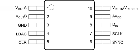
Pin Functions
| PIN | DESCRIPTION | |
|---|---|---|
| NAME | NO. | |
| AVDD | 9 | Power-supply input, 2.7 V to 5.5 V |
| CLR | 5 | Asynchronous clear input. The CLR input is falling-edge sensitive. When CLR is activated, zero scale (DACxx62-Q1) or mid-scale (DACxx63-Q1) is loaded to all input and DAC registers. This sets the DAC output voltages accordingly. The part exits clear code mode on the 24th falling edge of the next write to the part. If CLR is activated during a write sequence, the write is aborted. |
| DIN | 8 | Serial data input. Data are clocked into the 24-bit input shift register on each falling edge of the serial clock input. Schmitt-trigger logic input |
| GND | 3 | Ground reference point for all circuitry on the device |
| LDAC | 4 | In synchronous mode, data are updated with the falling edge of the 24th SCLK cycle, which follows a falling edge of SYNC. For such synchronous updates, the LDAC pin is not required, and it must be connected to GND permanently or asserted and held low before sending commands to the device. In asynchronous mode, the LDAC pin is used as a negative edge-triggered timing signal for simultaneous DAC updates. Multiple single-channel commands can be written in order to set different channel buffers to desired values and then make a falling edge on LDAC pin to simultaneously update the DAC output registers. |
| SCLK | 7 | Serial clock input. Data can be transferred at rates up to 50 MHz. Schmitt-trigger logic input |
| SYNC | 6 | Level-triggered control input (active-low). This input is the frame synchronization signal for the input data. When SYNC goes low, it enables the input shift register, and data are sampled on subsequent falling clock edges. The DAC output updates following the 24th clock falling edge. If SYNC is taken high before the 23rd clock edge, the rising edge of SYNC acts as an interrupt, and the write sequence is ignored by the DAC756x-Q1, DAC816x-Q1, DAC856x-Q1. Schmitt-trigger logic input |
| VOUTA | 1 | Analog output voltage from DAC-A |
| VOUTB | 2 | Analog output voltage from DAC-B |
| VREFIN/VREFOUT | 10 | Bidirectional voltage reference pin. If internal reference is used, 2.5-V output. |
7 Specifications
7.1 Absolute Maximum Ratings
Over operating free-air temperature range (unless otherwise noted).(1)| MIN | MAX | UNIT | ||
|---|---|---|---|---|
| AVDD to GND | –0.3 | 6 | V | |
| CLR, DIN, LDAC, SCLK and SYNC input voltage to GND | –0.3 | AVDD + 0.3 | V | |
| VOUT[A, B] to GND | –0.3 | AVDD + 0.3 | V | |
| VREFIN/VREFOUT to GND | –0.3 | AVDD + 0.3 | V | |
| Operating temperature | –40 | 125 | °C | |
| Junction temperature, TJ max | 150 | °C | ||
| Storage temperature, Tstg | –65 | 150 | °C | |
7.2 ESD Ratings
| VALUE | UNIT | ||||
|---|---|---|---|---|---|
| V(ESD) | Electrostatic discharge | Human-body model (HBM), per AEC Q100-002(1) | ±2000 | V | |
| Charged-device model (CDM), per AEC Q100-011 | All pins | ±500 | |||
| Corner pins (1, 5, 6, and 10) | ±750 | ||||
7.3 Recommended Operating Conditions
over operating free-air temperature range (unless otherwise noted)| MIN | NOM | MAX | UNIT | |||
|---|---|---|---|---|---|---|
| POWER SUPPLY | ||||||
| Supply voltage | AVDD to GND | 2.7 | 5.5 | V | ||
| DIGITAL INPUTS | ||||||
| Digital input voltage | CLR, DIN, LDAC, SCLK and SYNC | 0 | AVDD | V | ||
| REFERENCE INPUT | ||||||
| VREFIN | Reference input voltage | 0 | AVDD | V | ||
| TEMPERATURE RANGE | ||||||
| TA | Operating ambient temperature | –40 | 125 | °C | ||
7.4 Thermal Information
| THERMAL METRIC(1) | DACxx6x-Q1 | UNIT | |
|---|---|---|---|
| DGS (VSSOP) | |||
| 10 PINS | |||
| RθJA | Junction-to-ambient thermal resistance | 173.8 | °C/W |
| RθJC(top) | Junction-to-case (top) thermal resistance | 48.5 | °C/W |
| RθJB | Junction-to-board thermal resistance | 79.9 | °C/W |
| ψJT | Junction-to-top characterization parameter | 1.7 | °C/W |
| ψJB | Junction-to-board characterization parameter | 68.4 | °C/W |
7.5 Electrical Characteristics
At AVDD = 2.7 V to 5.5 V and TA = –40°C to 125°C (unless otherwise noted).| PARAMETER | TEST CONDITIONS | MIN | TYP | MAX | UNIT | ||
|---|---|---|---|---|---|---|---|
| STATIC PERFORMANCE(1) | |||||||
| DAC856x-Q1 | Resolution | 16 | Bits | ||||
| Relative accuracy | Using line passing through codes 512 and 65,024 | ±4 | ±12 | LSB | |||
| Differential nonlinearity | 16-bit monotonic | ±0.2 | ±1 | LSB | |||
| DAC816x-Q1 | Resolution | 14 | Bits | ||||
| Relative accuracy | Using line passing through codes 128 and 16,256 | ±1 | ±3 | LSB | |||
| Differential nonlinearity | 14-bit monotonic | ±0.1 | ±0.5 | LSB | |||
| DAC756x-Q1 | Resolution | 12 | Bits | ||||
| Relative accuracy | Using line passing through codes 32 and 4,064 | ±0.3 | ±0.75 | LSB | |||
| Differential nonlinearity | 12-bit monotonic | ±0.05 | ±0.25 | LSB | |||
| Offset error | Extrapolated from two-point line(1), unloaded | ±1 | ±4 | mV | |||
| Offset error drift | ±2 | µV/°C | |||||
| Full-scale error | DAC register loaded with all 1s | ±0.03 | ±0.2 | % FSR | |||
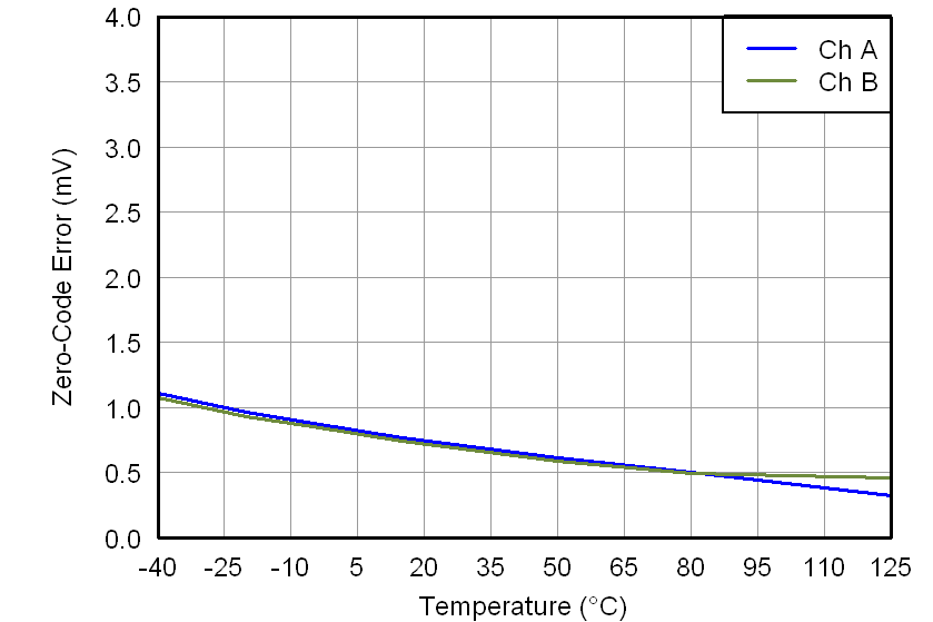
| Zero-code error | DAC register loaded with all 0s | 1 | 4 | mV | |||
| Zero-code error drift | ±2 | µV/°C | |||||
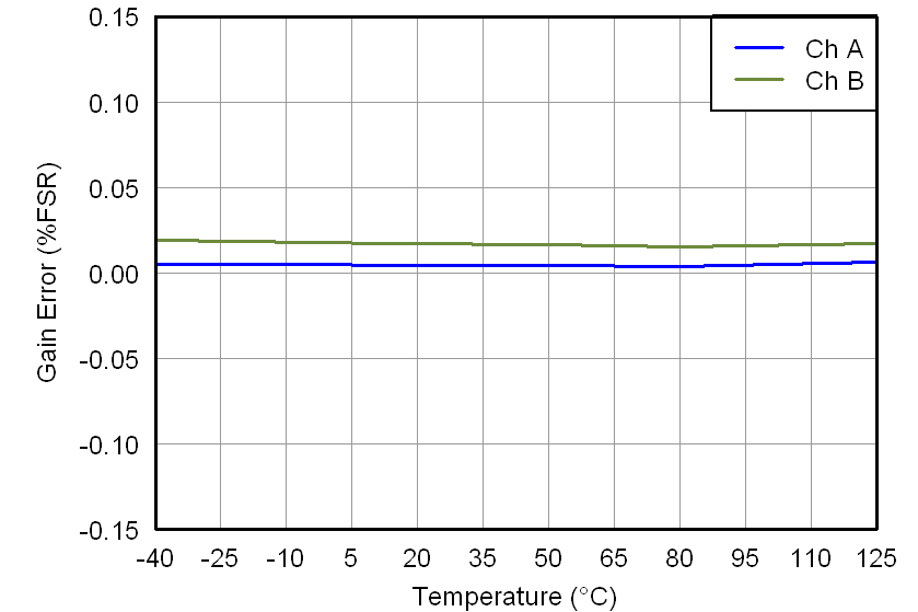
| Gain error | Extrapolated from two-point line(1), unloaded | ±0.01 | ±0.15 | % FSR | |||
| Gain temperature coefficient | ±1 | ppm FSR/°C | |||||
| OUTPUT CHARACTERISTICS(2) | |||||||
| Output voltage range | 0 | AVDD | V | ||||
| Output voltage settling time(3) | DACs unloaded | 7 | µs | ||||
| RL = 1 MΩ | 10 | ||||||
| Slew rate | Measured between 20% - 80% of a full-scale transition | 0.75 | V/µs | ||||
| Capacitive load stability | RL = ∞ | 1 | nF | ||||
| RL = 2 kΩ | 3 | ||||||
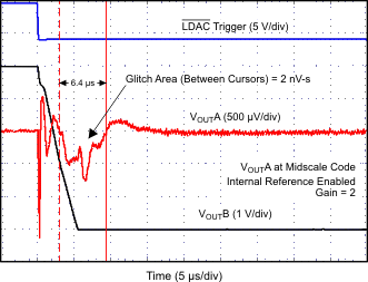
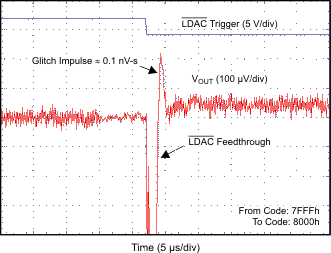
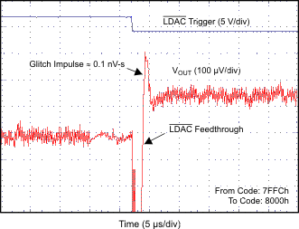
| Code-change glitch impulse | 1-LSB change around major carry | 0.1 | nV-s | ||||
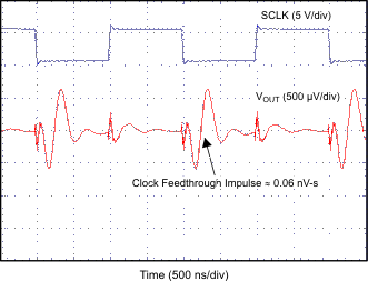
| Digital feedthrough | SCLK toggling, SYNC high | 0.1 | nV-s | ||||
| Power-on glitch impulse | RL = 2 kΩ, CL = 470 pF, AVDD = 5.5 V | 40 | mV | ||||
| Code-change total glitch amplitude | 1-LSB change around major carry. Includes glitch impulse and digital feedthrough. RL = 2 kΩ, CL = 470 pF, AVDD = 5.5 V |
3 | mV | ||||
| Channel-to-channel DC crosstalk | Full-scale swing on adjacent channel, External reference |
5 | µV | ||||
| Full-scale swing on adjacent channel, Internal reference |
15 | ||||||
| DC output impedance | At mid-scale input | 5 | Ω | ||||
| Short-circuit current | DAC outputs at full-scale, DAC outputs shorted to GND | 40 | mA | ||||
| Power-up time, including settling time | Coming out of power-down mode | 50 | µs | ||||
| AC PERFORMANCE(2) | |||||||
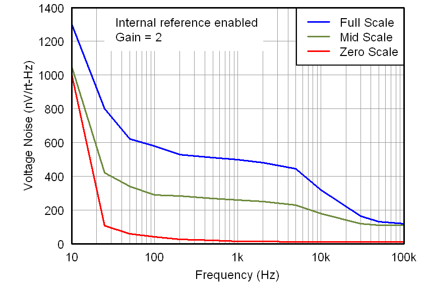
| DAC output noise density | TA = 25°C, at mid-scale input, fOUT = 1 kHz | 90 | nV/√Hz | ||||
| DAC output noise | TA = 25°C, at mid-scale input, 0.1 Hz to 10 Hz | 2.6 | µVPP | ||||
| LOGIC INPUTS(2) | |||||||
| Input pin Leakage current | –1 | ±0.1 | 1 | µA | |||
| Logic input LOW voltage VINL | 0 | 0.8 | V | ||||
| Logic input HIGH voltage VINH | 0.7 × AVDD | AVDD | V | ||||
| Pin capacitance | 3 | pF | |||||
| REFERENCE | |||||||
| External reference current | External VREF = 2.5 V (when internal reference is disabled), all channels active using gain = 1 | 15 | µA | ||||
| Reference input impedance | Internal reference disabled, gain = 1 | 170 | kΩ | ||||
| Internal reference disabled, gain = 2 | 85 | ||||||
| REFERENCE OUTPUT | |||||||
| Output voltage | TA = 25°C | 2.495 | 2.5 | 2.505 | V | ||
| Initial accuracy | TA = 25°C | –5 | ±0.1 | 5 | mV | ||
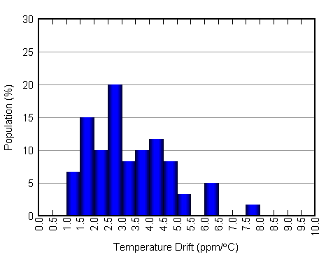
| Output voltage temperature drift | 4 | 10 | ppm/°C | ||||
| Output voltage noise | f = 0.1 Hz to 10 Hz | 12 | µVPP | ||||
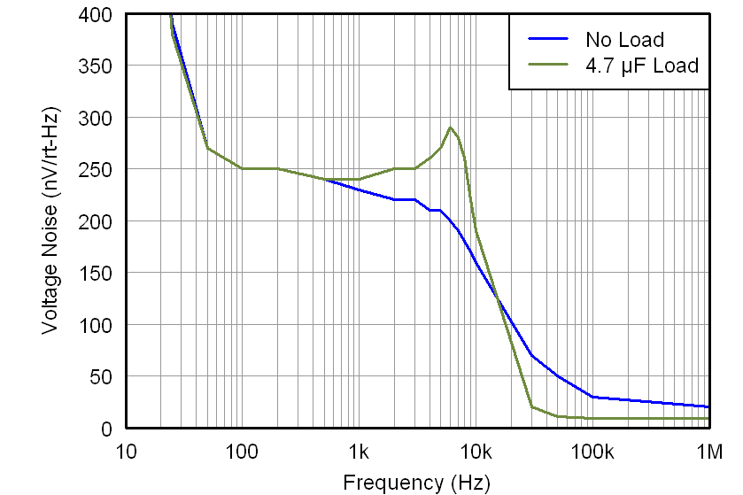
| Output voltage noise density (high-frequency noise) | TA = 25°C, f = 1 kHz, CL = 0 µF | 250 | nV/√Hz | ||||
| TA = 25°C, f = 1 MHz, CL = 0 µF | 30 | ||||||
| TA = 25°C, f = 1 MHz, CL = 4.7 µF | 10 | ||||||
| Load regulation, sourcing(4) | TA = 25°C | 20 | µV/mA | ||||
| Load regulation, sinking(4) | TA = 25°C | 185 | µV/mA | ||||
| Output current load capability(2) | ±20 | mA | |||||
| Line regulation | TA = 25°C | 50 | µV/V | ||||
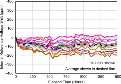
| Long-term stability and drift (aging)(4) | TA = 25°C, time = 0 to 1900 hours | 100 | ppm | ||||
| Thermal hysteresis(4) | First cycle | 200 | ppm | ||||
| Additional cycles | 50 | ||||||
| POWER REQUIREMENTS(5) | |||||||
| IDD | AVDD = 3.6 V to 5.5 V | Normal mode, internal reference off | 0.25 | 0.5 | mA | ||
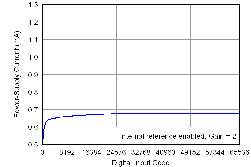
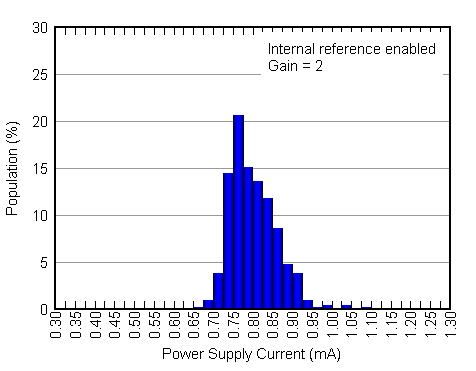
| Normal mode, internal reference on | 0.9 | 1.6 | |||||
| Power-down modes(6) | 0.55 | 2 | µA | ||||
| Power-down modes(7) | 0.55 | 4 | |||||
| AVDD = 2.7 V to 3.6 V | Normal mode, internal reference off | 0.2 | 0.4 | mA | |||
| Normal mode, internal reference on | 0.73 | 1.4 | |||||
| Power-down modes(6) | 0.35 | 2 | µA | ||||
| Power-down modes(7) | 0.35 | 3 | |||||
| Power dissipation | AVDD = 3.6 V to 5.5 V | Normal mode, internal reference off | 0.9 | 2.75 | mW | ||
| Normal mode, internal reference on | 3.2 | 8.8 | |||||
| Power-down modes(6) | 2 | 11 | µW | ||||
| Power-down modes(7) | 2 | 22 | |||||
| AVDD = 2.7 V to 3.6 V | Normal mode, internal reference off | 0.54 | 1.44 | mW | |||
| Normal mode, internal reference on | 1.97 | 5 | |||||
| Power-down modes(6) | 0.95 | 7.2 | µW | ||||
| Power-down modes(7) | 0.95 | 10.8 | |||||
7.6 Timing Requirements(1)(2)
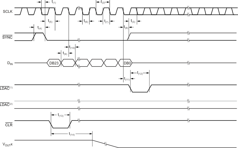
At AVDD = 2.7 V to 5.5 V and over –40°C to 125°C (unless otherwise noted). See Figure 1.| MIN | NOM | MAX | UNIT | ||
|---|---|---|---|---|---|
| f(SCLK) | Serial clock frequency | 50 | MHz | ||
| t1 | SCLK falling edge to SYNC falling edge (for successful write operation) | 10 | ns | ||
| t2 | SCLK cycle time | 20 | ns | ||
| t3 | SYNC rising edge to 23rd SCLK falling edge (for successful SYNC interrupt) | 13 | ns | ||
| t4 | Minimum SYNC HIGH time | 80 | ns | ||
| t5 | SYNC to SCLK falling edge setup time | 13 | ns | ||
| t6 | SCLK LOW time | 8 | ns | ||
| t7 | SCLK HIGH time | 8 | ns | ||
| t8 | SCLK falling edge to SYNC rising edge | 10 | ns | ||
| t9 | Data setup time | 6 | ns | ||
| t10 | Data hold time | 5 | ns | ||
| t11 | SCLK falling edge to LDAC falling edge for asynchronous LDAC update mode | 5 | ns | ||
| t12 | LDAC pulse duration, LOW time | 10 | ns | ||
| t13 | CLR pulse duration, LOW time | 80 | ns | ||
| t14 | CLR falling edge to start of VOUT transition | 100 | ns | ||
7.7 Typical Characteristics
7.7.1 Tables of Graphs
Table 1. Typical Characteristics: Internal Reference Performance
| MEASUREMENT | POWER-SUPPLY VOLTAGE | FIGURE NUMBER | |
|---|---|---|---|
| Internal Reference Voltage vs Temperature | 5.5 V | Figure 2 | |
| Internal Reference Voltage Temperature Drift Histogram | Figure 3 | ||
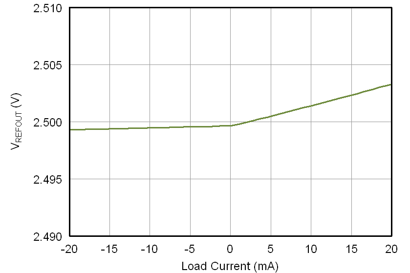
| Internal Reference Voltage vs Load Current | Figure 4 | ||
| Internal Reference Voltage vs Time | Figure 5 | ||
| Internal Reference Noise Density vs Frequency | Figure 6 | ||
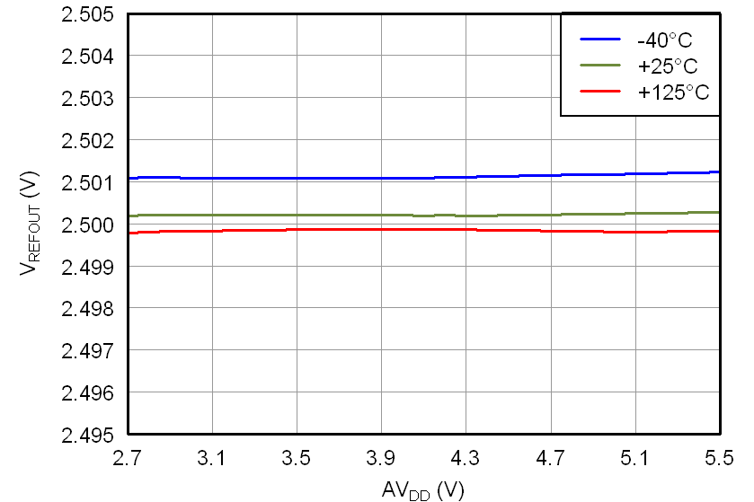
| Internal Reference Voltage vs Supply Voltage | 2.7 V – 5.5 V | Figure 7 | |
Table 2. Typical Characteristics: DAC Static Performance
| MEASUREMENT | POWER-SUPPLY VOLTAGE | FIGURE NUMBER | |
|---|---|---|---|
| FULL-SCALE, GAIN, OFFSET AND ZERO-CODE ERRORS | |||
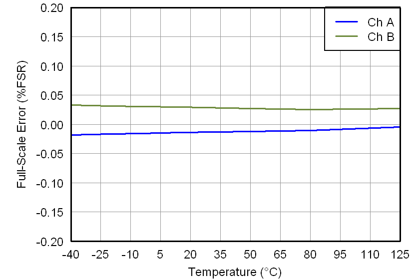
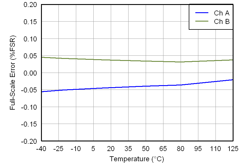
| Full-Scale Error vs Temperature | 5.5 V | Figure 16 | |
| Gain Error vs Temperature | Figure 17 | ||
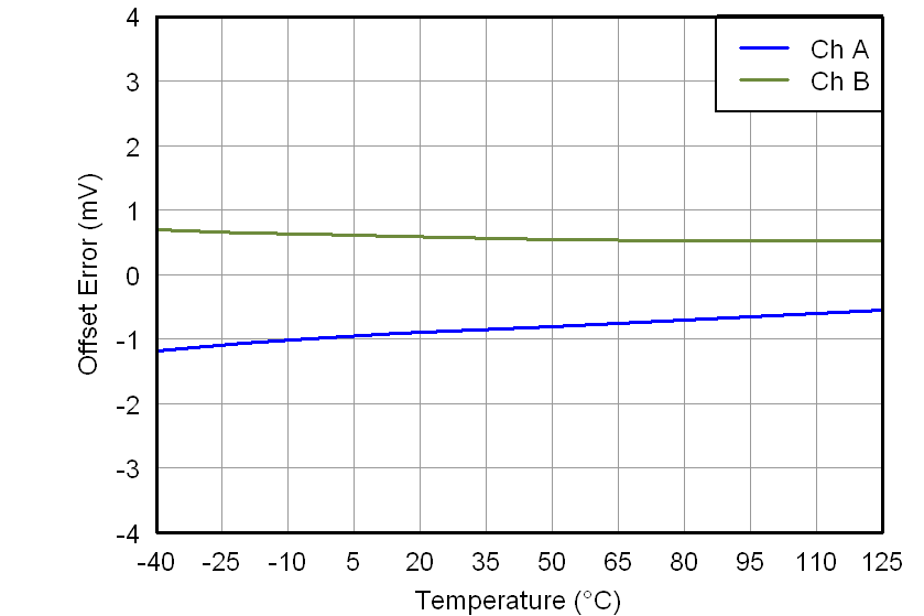
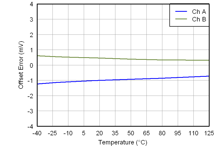
| Offset Error vs Temperature | Figure 18 | ||
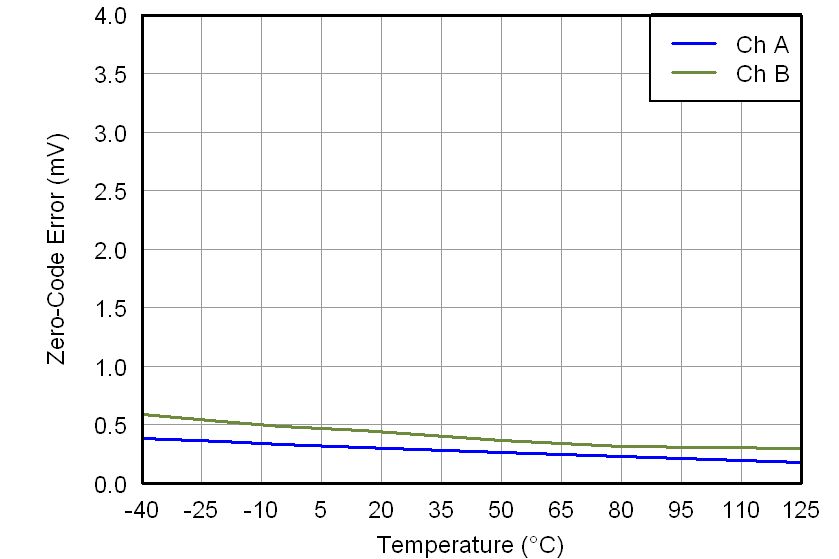
| Zero-Code Error vs Temperature | Figure 19 | ||
| Full-Scale Error vs Temperature | 2.7 V | Figure 63 | |
| Gain Error vs Temperature | Figure 64 | ||
| Offset Error vs Temperature | Figure 65 | ||
| Zero-Code Error vs Temperature | Figure 66 | ||
| LOAD REGULATION | |||
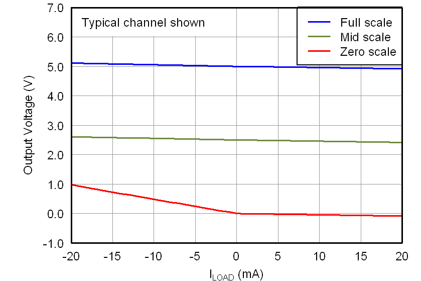
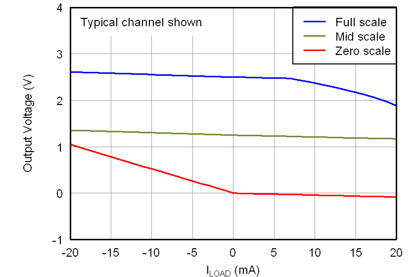
| DAC Output Voltage vs Load Current | 5.5 V | Figure 30 | |
| 2.7 V | Figure 74 | ||
| DIFFERENTIAL NONLINEARITY ERROR | |||
| Differential Linearity Error vs Digital Input Code | T = –40°C | 5.5 V | Figure 9 |
| T = 25°C | Figure 11 | ||
| T = 125°C | Figure 13 | ||
| Differential Linearity Error vs Temperature | Figure 15 | ||
| Differential Linearity Error vs Digital Input Code | T = –40°C | 2.7 V | Figure 56 |
| T = 25°C | Figure 58 | ||
| T = 125°C | Figure 60 | ||
| Differential Linearity Error vs Temperature | Figure 62 | ||
| INTEGRAL NONLINEARITY ERROR (RELATIVE ACCURACY) | |||
| Linearity Error vs Digital Input Code | T = –40°C | 5.5 V | Figure 8 |
| T = 25°C | Figure 10 | ||
| T = 125°C | Figure 12 | ||
| Linearity Error vs Temperature | Figure 14 | ||
| Linearity Error vs Digital Input Code | T = –40°C | 2.7 V | Figure 55 |
| T = 25°C | Figure 57 | ||
| T = 125°C | Figure 59 | ||
| Linearity Error vs Temperature | Figure 61 | ||
| POWER-DOWN CURRENT | |||
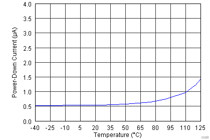
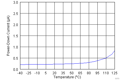
| Power-Down Current vs Temperature | 5.5 V | Figure 28 | |
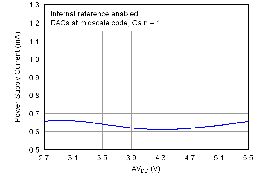
| Power-Down Current vs Power-Supply Voltage | 2.7 V – 5.5 V | Figure 29 | |
| Power-Down Current vs Temperature | 2.7 V | Figure 73 | |
| POWER-SUPPLY CURRENT | |||
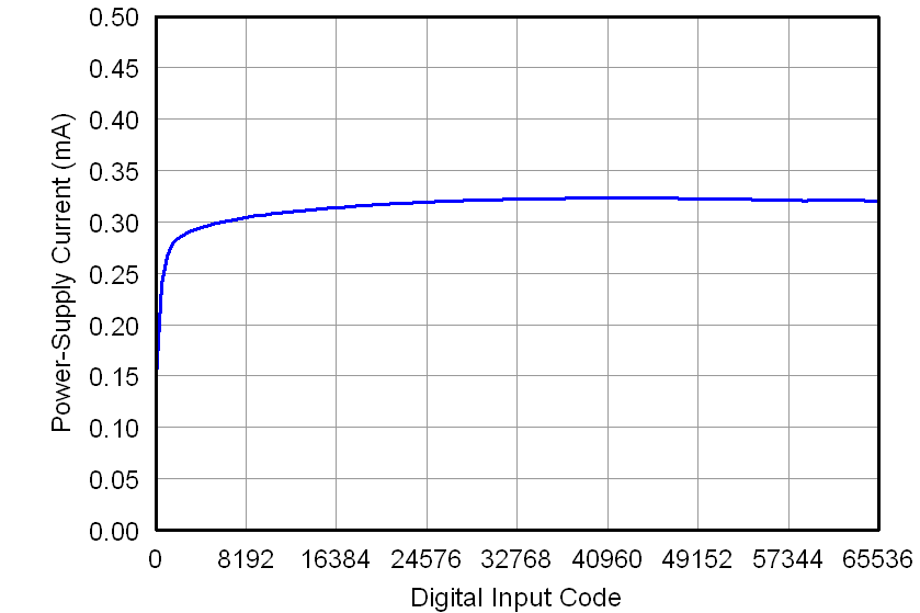
| Power-Supply Current vs Temperature | External VREF | 5.5 V | Figure 20 |
| Internal VREF | Figure 21 | ||
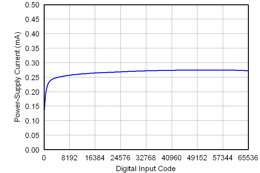
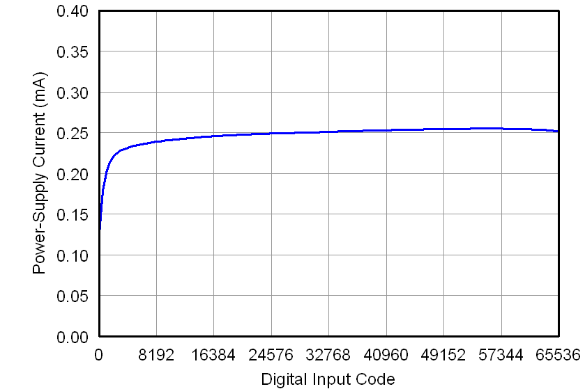
| Power-Supply Current vs Digital Input Code | External VREF | Figure 22 | |
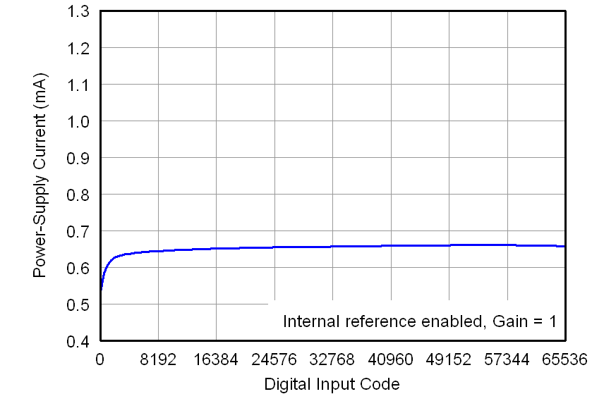
| Internal VREF | Figure 23 | ||
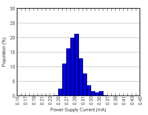
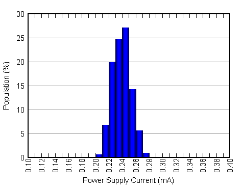
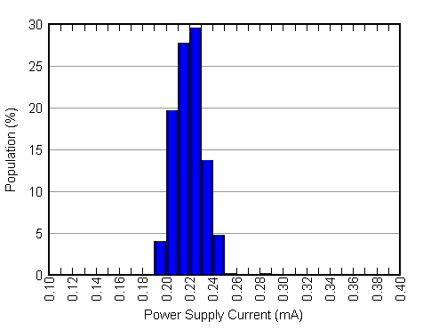
| Power-Supply Current Histogram | External VREF | Figure 24 | |
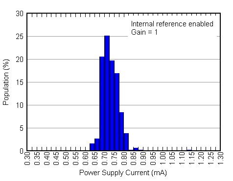
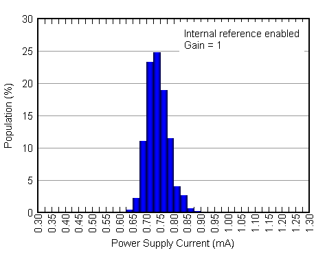
| Internal VREF | Figure 25 | ||
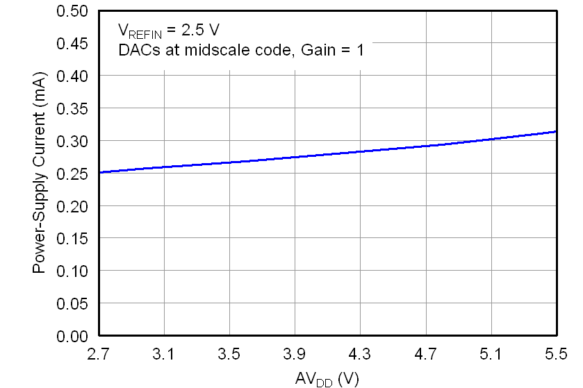
| Power-Supply Current vs Power-Supply Voltage | External VREF | 2.7 V – 5.5 V | Figure 26 |
| Internal VREF | Figure 27 | ||
| Power-Supply Current vs Temperature | External VREF | 3.6 V | Figure 49 |
| Internal VREF | Figure 50 | ||
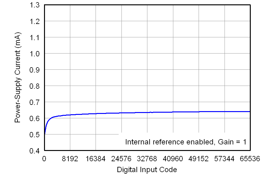
| Power-Supply Current vs Digital Input Code | External VREF | Figure 51 | |
| Internal VREF | Figure 52 | ||
| Power-Supply Current Histogram | External VREF | Figure 53 | |
| Internal VREF | Figure 54 | ||
| Power-Supply Current vs Temperature | External VREF | 2.7 V | Figure 67 |
| Internal VREF | Figure 68 | ||
| Power-Supply Current vs Digital Input Code | External VREF | Figure 69 | |
| Internal VREF | Figure 70 | ||
| Power-Supply Current Histogram | External VREF | Figure 71 | |
| Internal VREF | Figure 72 | ||
Table 3. Typical Characteristics: DAC Dynamic Performance
| MEASUREMENT | POWER-SUPPLY VOLTAGE | FIGURE NUMBER | |
|---|---|---|---|
| CHANNEL-TO-CHANNEL CROSSTALK | |||
| Channel-to-Channel Crosstalk | 5-V Rising Edge | 5.5 V | Figure 43 |
| 5-V Falling Edge | Figure 44 | ||
| CLOCK FEEDTHROUGH | |||
| Clock Feedthrough | 500 kHz, Mid-Scale | 5.5 V | Figure 48 |
| 2.7 V | Figure 87 | ||
| GLITCH IMPULSE | |||
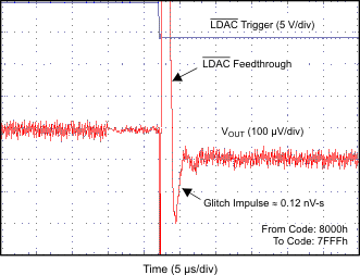
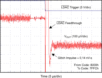
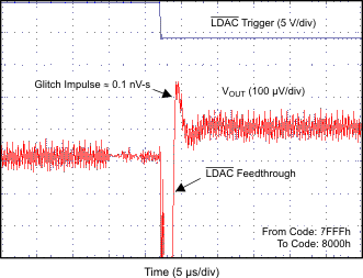
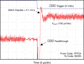
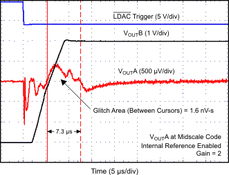
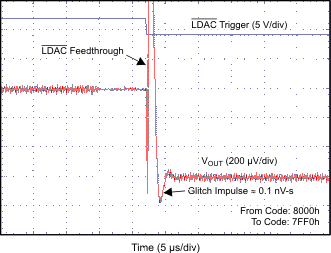
| Glitch Impulse, 1-LSB Step | Rising Edge, Code 7FFFh to 8000h | 5.5 V | Figure 37 |
| Falling Edge, Code 8000h to 7FFFh | Figure 38 | ||
| Glitch Impulse, 4-LSB Step | Rising Edge, Code 7FFCh to 8000h | Figure 39 | |
| Falling Edge, Code 8000h to 7FFCh | Figure 40 | ||
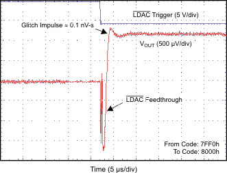
| Glitch Impulse, 16-LSB Step | Rising Edge, Code 7FF0h to 8000h | Figure 41 | |
| Falling Edge, Code 8000h to 7FF0h | Figure 42 | ||
| Glitch Impulse, 1-LSB Step | Rising Edge, Code 7FFFh to 8000h | 2.7 V | Figure 79 |
| Falling Edge, Code 8000h to 7FFFh | Figure 80 | ||
| Glitch Impulse, 4-LSB Step | Rising Edge, Code 7FFCh to 8000h | Figure 81 | |
| Falling Edge, Code 8000h to 7FFCh | Figure 82 | ||
| Glitch Impulse, 16-LSB Step | Rising Edge, Code 7FF0h to 8000h | Figure 83 | |
| Falling Edge, Code 8000h to 7FF0h | Figure 84 | ||
| NOISE | |||
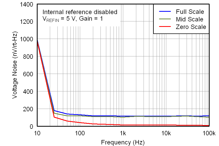
| DAC Output Noise Density vs Frequency | External VREF | 5.5 V | Figure 45 |
| Internal VREF | Figure 46 | ||
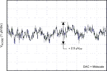
| DAC Output Noise 0.1 Hz to 10 Hz | External VREF | Figure 47 | |
| POWER-ON GLITCH | |||
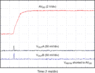
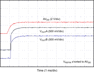
| Power-on Glitch | Reset to Zero Scale | 5.5 V | Figure 35 |
| Reset to Mid-Scale | Figure 36 | ||
| Reset to Zero Scale | 2.7 V | Figure 85 | |
| Reset to Mid-Scale | Figure 86 | ||
| SETTLING TIME | |||
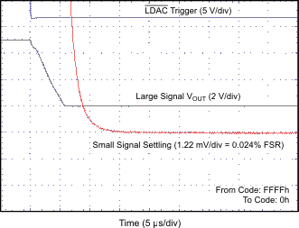
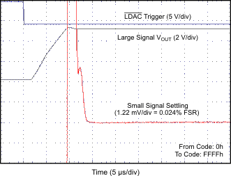
| Full-Scale Settling Time | Rising Edge, Code 0h to FFFFh | 5.5 V | Figure 31 |
| Falling Edge, Code FFFFh to 0h | Figure 32 | ||
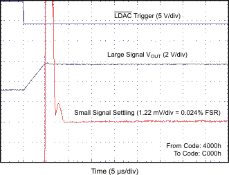
| Half-Scale Settling Time | Rising Edge, Code 4000h to C000h | Figure 33 | |
| Falling Edge, Code C000h to 4000h | Figure 34 | ||
| Full-Scale Settling Time | Rising Edge, Code 0h to FFFFh | 2.7 V | Figure 75 |
| Falling Edge, Code FFFFh to 0h | Figure 76 | ||
| Half-Scale Settling Time | Rising Edge, Code 4000h to C000h | Figure 77 | |
| Falling Edge, Code C000h to 4000h | Figure 78 | ||
7.7.2 Internal Reference
At TA = 25°C, AVDD = 5.5 V, gain = 2 and VREFOUT, unloaded unless otherwise noted.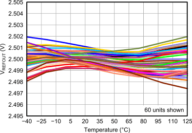
7.7.3 DAC at AVDD = 5.5 V
At TA = 25°C, 5-V external reference used, gain = 1 and DAC output not loaded, unless otherwise noted..png)
.png)
.png)
.png)
.png)
.png)
.png)
.png)
.png)
.png)
7.7.4 Typical Characteristics: DAC at AVDD = 3.6 V
At TA = 25°C, 3.3-V external reference used, gain = 1 and DAC output not loaded, unless otherwise noted..png)
.png)
7.7.5 Typical Characteristics: DAC at AVDD = 2.7 V
At TA = 25°C, 2.5-V external reference used, gain = 1 and DAC output not loaded, unless otherwise noted..png) Figure 55. Linearity Error vs Digital Input Code (–40°C)
Figure 55. Linearity Error vs Digital Input Code (–40°C)
.png) Figure 57. Linearity Error vs Digital Input Code (25°C)
Figure 57. Linearity Error vs Digital Input Code (25°C)
.png) Figure 59. Linearity Error vs Digital Input Code (125°C)
Figure 59. Linearity Error vs Digital Input Code (125°C)
.png)
.png)
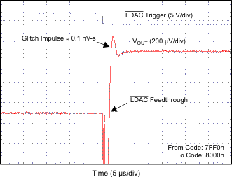
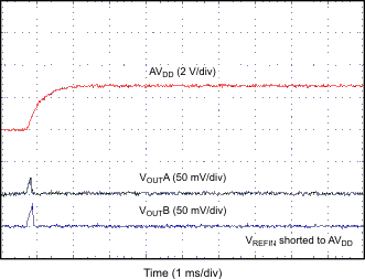
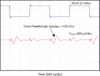
.png) Figure 56. Differential Linearity Error vs Digital Input Code (–40°C)
Figure 56. Differential Linearity Error vs Digital Input Code (–40°C)
.png) Figure 58. Differential Linearity Error vs Digital Input Code (25°C)
Figure 58. Differential Linearity Error vs Digital Input Code (25°C)
.png) Figure 60. Differential Linearity Error vs Digital Input Code (125°C)
Figure 60. Differential Linearity Error vs Digital Input Code (125°C)
.png)
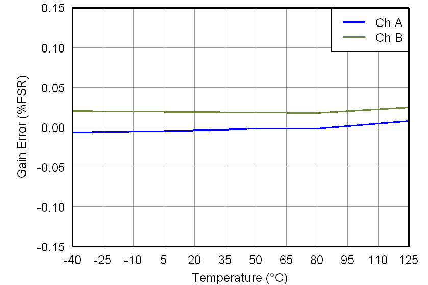
.png)
8 Detailed Description
8.1 Overview
The DAC756x-Q1, DAC816x-Q1, and DAC856x-Q1 devices are low-power, voltage-output, dual-channel, 12-, 14-, and 16-bit digital-to-analog converters (DACs), respectively. These devices include a 2.5-V, 4-ppm/°C internal reference, giving a full-scale output voltage range of 2.5 V or 5 V. The internal reference has an initial accuracy of ±5 mV and can source or sink up to 20 mA at the VREFIN/VREFOUT pin.
8.2 Functional Block Diagram

8.3 Feature Description
8.3.1 Digital-to-Analog Converter (DAC)
The DAC756x-Q1, DAC816x-Q1, and DAC856x-Q1 architecture consists of two string DACs, each followed by an output buffer amplifier. The devices include an internal 2.5-V reference with 4-ppm/°C temperature drift performance. Figure 88 shows a principal block diagram of the DAC architecture.
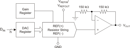 Figure 88. DAC Architecture
The input coding to the DAC756x-Q1, DAC816x-Q1, and DAC856x-Q1 devices is straight binary, so the ideal output voltage is given by Equation 1:

where:
n = resolution in bits; either 12 (DAC756x-Q1), 14 (DAC816x-Q1) or 16 (DAC856x-Q1)
DIN = decimal equivalent of the binary code that is loaded to the DAC register. DIN ranges from 0 to 2n – 1.
VREF = DAC reference voltage; either VREFOUT from the internal 2.5-V reference or VREFIN from an
aaa external reference.
Gain = 1 by default when internal reference is disabled (using external reference), and gain = 2 by default
aaa when using internal reference. Gain can also be manually set to either 1 or 2 using the gain register.
aaa See the Gain Function section for more information.
8.3.1.1 Resistor String
The resistor string section is shown in Figure 89. It is simply a string of resistors, each of value R. The code loaded into the DAC register determines at which node on the string the voltage is tapped off to be fed into the output amplifier by closing one of the switches connecting the string to the amplifier. The resistor string architecture results in monotonicity. The RDIVIDER switch is controlled by the gain registers (see the Gain Function section). Because the output amplifier has a gain of 2, RDIVIDER is not shorted when the DAC-n gain is set to 1 (default if internal reference is disabled), and is shorted when the DAC-n gain is set to 2 (default if internal reference is enabled).
 Figure 89. Resistor String
8.3.1.2 Output Amplifier
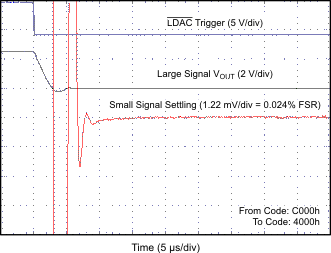
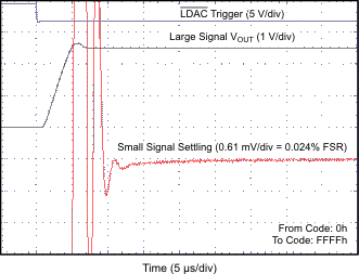
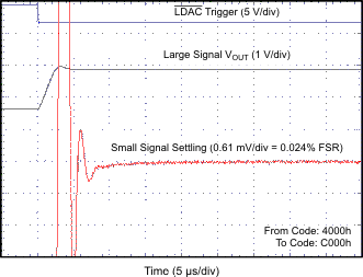
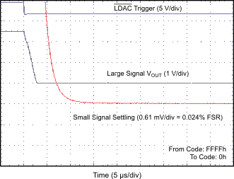
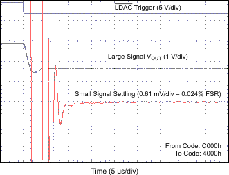
The output buffer amplifier is capable of generating rail-to-rail voltages on its output, giving a maximum output range of 0 V to AVDD. It is capable of driving a load of 2 kΩ in parallel with 3 nF to GND. The typical slew rate is 0.75 V/µs, with a typical full-scale settling time of 14 µs as shown in Figure 31, Figure 32, Figure 75 and Figure 76.
8.3.2 Internal Reference
The DAC756x-Q1, DAC816x-Q1, and DAC856x-Q1 devices include a 2.5-V internal reference that is disabled by default. The internal reference is externally available at the VREFIN/VREFOUT pin. The internal reference output voltage is 2.5 V and can sink and source up to 20 mA.
A minimum 150-nF capacitor is recommended between the reference output and GND for noise filtering.
The internal reference of the DAC756x-Q1, DAC816x-Q1, and DAC856x-Q1 devices is a bipolar transistor-based precision band-gap voltage reference. Figure 90 shows the basic band-gap topology. Transistors Q1 and Q2 are biased such that the current density of Q1 is greater than that of Q2. The difference of the two base-emitter voltages (VBE1 – VBE2) has a positive temperature coefficient and is forced across resistor R1. This voltage is amplified and added to the base-emitter voltage of Q2, which has a negative temperature coefficient. The resulting output voltage is virtually independent of temperature. The short-circuit current is limited by design to approximately 100 mA.
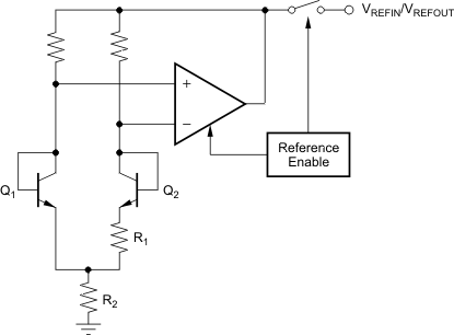 Figure 90. Band-Gap Reference Simplified Schematic
8.3.3 Power-On Reset
8.3.3.1 Power-On Reset to Zero-Scale
The DAC7562-Q1, DAC8162-Q1, and DAC8562-Q1 devices contain a power-on-reset circuit that controls the output voltage during power up. All device registers are reset as shown in Table 4. At power up, all DAC registers are filled with zeros and the output voltages of all DAC channels are set to zero volts. Each DAC channel remains that way until a valid load command is written to it. The power-on reset is useful in applications where it is important to know the state of the output of each DAC while the device is in the process of powering up. No device pin should be brought high before applying power to the device. The internal reference is disabled by default and remains that way until a valid reference-change command is executed.
8.3.3.2 Power-On Reset to Mid-Scale
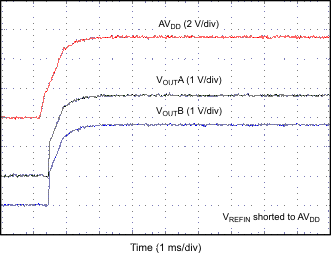
The DAC7563-Q1, DAC8163-Q1, and DAC8563-Q1 devices contain a power-on reset circuit that controls the output voltage during power up. At power up, all DAC registers are reset to mid-scale code and the output voltages of all DAC channels are set to VREFIN / 2 V. Each DAC channel remains that way until a valid load command is written to it. The power-on reset is useful in applications where it is important to know the state of the output of each DAC while the device is in the process of powering up. No device pin should be brought high before applying power to the device. The internal reference is powered off or down by default and remains that way until a valid reference-change command is executed. If using an external reference, it is acceptable to power on the VREFIN pin either at the same time as or after applying AVDD.
Table 4. DACxx62-Q1 and DACxx63-Q1 Power-On Reset Values
| REGISTER | DEFAULT SETTING | |
|---|---|---|
| DAC and input registers | DACxx62-Q1 | Zero-scale |
| DACxx63-Q1 | Mid-scale | |
| LDAC registers | LDAC pin enabled for both channels | |
| Power-down registers | DACs powered up | |
| Internal reference register | Internal reference disabled | |
| Gain registers | Gain = 1 for both channels | |
8.3.3.3 Power-On Reset (POR) Levels
When the device powers up, a POR circuit sets the device in default mode as shown in Table 4. The POR circuit requires specific AVDD levels, as indicated in Figure 91, to ensure discharging of internal capacitors and to reset the device on power up. In order to ensure a power-on reset, AVDD must be below 0.7 V for at least 1 ms. When AVDD drops below 2.2 V but remains above 0.7 V (shown as the undefined region), the device may or may not reset under all specified temperature and power-supply conditions. In this case, TI recommends a power-on reset. When AVDD remains above 2.2 V, a power-on reset does not occur.
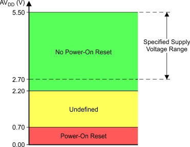 Figure 91. Relevant Voltage Levels for POR Circuit
8.4 Device Functional Modes
8.4.1 Power-Down Modes
The DAC756x-Q1, DAC816x-Q1, and DAC856x-Q1 devices have two separate sets of power-down commands. One set is for the DAC channels and the other set is for the internal reference. The internal reference is forced to a powered-down state while both DAC channels are powered down, and is only enabled if any DAC channel is also in the normal mode of operation. For more information on the internal reference control, see the Internal Reference Enable Register section.
8.4.1.1 DAC Power-Down Commands
The DAC756x-Q1, DAC816x-Q1, and DAC856x-Q1 DACs use four modes of operation. These modes are accessed by setting the serial interface command bits to 100. Once the command bits are set correctly, the four different power-down modes are software programmable by setting bits DB5 and DB4 in the shift register. Table 5 and Table 6 show the different power-down options. For more information on how to set the DAC operating mode see Table 17.
Table 5. DAC-n Operating Modes
| DB5 | DB4 | DAC MODES OF OPERATION |
|---|---|---|
| 0 | 0 | Selected DACs power up (normal mode, default) |
| 0 | 1 | Selected DACs power down, output 1 kΩ to GND |
| 1 | 0 | Selected DACs power down, output 100 kΩ to GND |
| 1 | 1 | Selected DACs power down, output Hi-Z to GND |
Table 6. DAC-n Selection for Operating Modes
| DAC-B (DB1), DAC-A (DB0) | OPERATING MODE |
|---|---|
| 0 | DAC-n does not change operating mode |
| 1 | DAC-n operating mode set to value on PD1 and PD0 |
It is possible to write to the DAC register or buffer of the DAC channel that is powered down. When the DAC channel is then powered up, it powers up to this new value.
The advantage of the available power-down modes is that the output impedance of the device is known while it is in power-down mode. As described in Table 5, there are three different power-down options. VOUT can be connected internally to GND through a 1-kΩ resistor, a 100-kΩ resistor, or open-circuited (Hi-Z). The DAC power-down circuitry is shown in Figure 92.
 Figure 92. Output Stage
8.4.2 Gain Function
The gain register controls the GAIN setting in the DAC transfer function:

The DAC756x-Q1, DAC816x-Q1, and DAC856x-Q1 devices have a gain register for each channel. The gain for each channel, in Equation 2, is either 1 or 2. This gain is automatically set to 2 when using the internal reference, and is automatically set to 1 when the internal reference is disabled (default). However, each channel can have either gain by setting the registers appropriately. The gain registers are accessible by setting the serial interface command bits to 000, address bits to 010, and using DB1 for DAC-B and DB0 for DAC-A. See Table 7 and Table 17 for the full command structure. The gain registers are automatically reset to provide either gain of 1 or 2 when the internal reference is powered off or on, respectively. After the reference is powered off or on, the gain register is again accessible to change the gain.
Table 7. DAC-n Selection for Gain Register Command
| DB1, DB0 | VALUE | GAIN |
|---|---|---|
| DB0 | 0 | DAC-A uses gain = 2 (default with internal reference) |
| 1 | DAC-A uses gain = 1 (default with external reference) | |
| DB1 | 0 | DAC-B uses gain = 2 (default with internal reference) |
| 1 | DAC-B uses gain = 1 (default with external reference) |
8.4.3 Software Reset Function
The DAC756x-Q1, DAC816x-Q1, and DAC856x-Q1 devices contain a software reset feature. The software reset function is accessed by setting the serial interface command bits to 101. The software reset command contains two reset modes which are software-programmable by setting bit DB0 in the shift register. Table 8 and Table 17 show the available software reset commands.
Table 8. Software Reset
| DB0 | REGISTERS RESET TO DEFAULT VALUES |
|---|---|
| 0 | DAC registers Input registers |
| 1 | DAC registers Input registers LDAC registers Power-down registers Internal reference register Gain registers |
8.4.4 Internal Reference Enable Register
The internal reference in the DAC756x-Q1, DAC816x-Q1, and DAC856x-Q1 devices is disabled by default for debugging, evaluation purposes, or when using an external reference. The internal reference can be powered up and powered down by setting the serial interface command bits to 111 and configuring DB0 (see Table 9). The internal reference is forced to a powered down state while both DAC channels are powered down, and can only be enabled if any DAC channel is in normal mode of operation. During the time that the internal reference is disabled, the DAC functions normally using an external reference. At this point, the internal reference is disconnected from the VREFIN/VREFOUT pin (Hi-Z output).
Table 9. Internal Reference
| DB0 | INTERNAL REFERENCE CONFIGURATION |
|---|---|
| 0 | Disable internal reference and reset DACs to gain = 1 |
| 1 | Enable internal reference and reset DACs to gain = 2 |
8.4.4.1 Enabling Internal Reference
To enable the internal reference, refer to the command structure in Table 17. When performing a power cycle to reset the device, the internal reference is switched off (default mode). In the default mode, the internal reference is powered down until a valid write sequence powers up the internal reference. However, the internal reference is forced to a disabled state while both DAC channels are powered down, and remains disabled until either DAC channel is returned to the normal mode of operation. See DAC Power-Down Commands for more information on DAC channel modes of operation.
8.4.4.2 Disabling Internal Reference
To disable the internal reference, refer to the command structure in Table 17. When performing a power cycle to reset the device, the internal reference is disabled (default mode).
8.4.5 CLR Functionality
The edge-triggered CLR pin can be used to set the input and DAC registers immediately according to Table 10. When the CLR pin receives a falling edge signal the clear mode is activated and changes the DAC output voltages accordingly. The device exits clear mode on the 24th falling edge of the next write to the device. If the CLR pin receives a falling edge signal during a write sequence in normal operation, the clear mode is activated and changes the input and DAC registers immediately according to Table 10.
Table 10. Clear Mode Reset Values
| DEVICE | DAC OUTPUT ENTERING CLEAR MODE |
|---|---|
| DAC8562-Q1, DAC8162-Q1, DAC7562-Q1 | Zero-scale |
| DAC8563-Q1, DAC8163-Q1, DAC7563-Q1 | Mid-scale |
8.4.6 LDAC Functionality
The DAC756x-Q1, DAC816x-Q1, and DAC856x-Q1 devices offer both a software and hardware simultaneous update and control function. The DAC double-buffered architecture has been designed so that new data can be entered for each DAC without disturbing the analog outputs.
DAC756x-Q1, DAC816x-Q1, and DAC856x-Q1 data updates can be performed either in synchronous or in asynchronous mode.
In asynchronous mode, the LDAC pin is used as a negative edge-triggered timing signal for simultaneous DAC updates. Multiple single-channel writes can be done in order to set different channel buffers to desired values and then make a falling edge on LDAC pin to simultaneously update the DAC output registers. Data buffers of all channels must be loaded with desired data before an LDAC falling edge. After a high-to-low LDAC transition, all DACs are simultaneously updated with the last contents of the corresponding data buffers. If the content of a data buffer is not changed, the corresponding DAC output remains unchanged after the LDAC pin is triggered. LDAC must be returned high before the next serial command is initiated.
In synchronous mode, data are updated with the falling edge of the 24th SCLK cycle, which follows a falling edge of SYNC. For such synchronous updates, the LDAC pin is not required, and it must be connected to GND permanently or asserted and held low before sending commands to the device.
Alternatively, all DAC outputs can be updated simultaneously using the built-in software function of LDAC. The LDAC register offers additional flexibility and control by allowing the selection of which DAC channel(s) should be updated simultaneously when the LDAC pin is being brought low. The LDAC register is loaded with a 2-bit word (DB1 and DB0) using command bits C2, C1, and C0 (see Table 17). The default value for each bit, and therefore for each DAC channel, is zero. If the LDAC register bit is set to 1, it overrides the LDAC pin (the LDAC pin is internally tied low for that particular DAC channel) and this DAC channel updates synchronously after the falling edge of the 24th SCLK cycle. However, if the LDAC register bit is set to 0, the DAC channel is controlled by the LDAC pin.
The combination of software and hardware simultaneous update functions is particularly useful in applications when updating a DAC channel, while keeping the other channel unaffected; see Table 11 and Table 17 for more information.
Table 11. DAC-n Selection for LDAC Register Command
| DB1, DB0 | VALUE | LDAC PIN FUNCTIONALITY |
|---|---|---|
| DB0 | 0 | DAC-A uses LDAC pin |
| 1 | DAC-A operates in synchronous mode | |
| DB1 | 0 | DAC-B uses LDAC pin |
| 1 | DAC-B operates in synchronous mode |
8.5 Programming
The DAC756x-Q1, DAC816x-Q1, and DAC856x-Q1 devices have a three-wire serial interface (SYNC, SCLK, and DIN; see the table) compatible with SPI, QSPI, and Microwire interface standards, as well as most DSPs. See the Serial Write Operation timing diagram (Figure 1) for an example of a typical write sequence.
The DAC756x-Q1, DAC816x-Q1, or DAC856x-Q1 input shift register is 24 bits wide, consisting of two don’t care bits (DB23 to DB22), three command bits (DB21 to DB19), three address bits (DB18 to DB16), and 16 data bits (DB15 to DB0). All 24 bits of data are loaded into the DAC under the control of the serial clock input, SCLK. DB23 (MSB) is the first bit that is loaded into the DAC shift register. DB23 is followed by the rest of the 24-bit word pattern, left-aligned. This configuration means that the first 24 bits of data are latched into the shift register, and any further clocking of data is ignored.
The write sequence begins by bringing the SYNC line low. Data from the DIN line are clocked into the 24-bit shift register on each falling edge of SCLK. The serial clock frequency can be as high as 50 MHz, making the DAC756x-Q1, DAC816x-Q1, and DAC856x-Q1 devices compatible with high-speed DSPs. On the 24th falling edge of the serial clock, the last data bit is clocked into the shift register and the shift register locks. Further clocking does not change the shift register data.
After receiving the 24th falling clock edge, the DAC756x-Q1, DAC816x-Q1, and DAC856x-Q1 devices decode the three command bits, three address bits and 16 data bits to perform the required function, without waiting for a SYNC rising edge. After the 24th falling edge of SCLK is received, the SYNC line may be kept low or brought high. In either case, the minimum delay time from the 24th falling SCLK edge to the next falling SYNC edge must be met in order to begin the next cycle properly; see the Serial Write Operation timing diagram (Figure 1).
A rising edge of SYNC before the 24-bit sequence is complete resets the SPI interface; no data transfer occurs. A new write sequence starts at the next falling edge of SYNC. To assure the lowest power consumption of the device, care should be taken that the levels are as close to each rail as possible.
8.5.1 SYNC Interrupt
In a normal write sequence, the SYNC line stays low for at least 24 falling edges of SCLK and the addressed DAC register updates on the 24th falling edge. However, if SYNC is brought high before the 23rd falling edge, it acts as an interrupt to the write sequence; the shift register resets and the write sequence is discarded. Neither an update of the data buffer contents, DAC register contents, nor a change in the operating mode occurs (as shown in Figure 93).
 Figure 93. SYNC Interrupt Facility
8.5.2 DAC Register Configuration
When the DAC registers are being written to, the DAC756x-Q1, DAC816x-Q1, and DAC856x-Q1 devices receive all 24 bits of data, ignore DB23 and DB22, and decode the next three bits (DB21 to DB19) in order to determine the DAC operating or control mode (see Table 12). Bits DB18 to DB16 are used to address the DAC channels (see Table 13).
Table 12. Commands for the DAC756x-Q1, DAC816x-Q1, and DAC856x-Q1 Devices
| C2 (DB21) |
C1 (DB20) |
C0 (DB19) |
COMMAND |
|---|---|---|---|
| 0 | 0 | 0 | Write to input register n (Table 13) |
| 0 | 0 | 1 | Software LDAC, update DAC register n (Table 13) |
| 0 | 1 | 0 | Write to input register n (Table 13) and update all DAC registers |
| 0 | 1 | 1 | Write to input register n and update DAC register n (Table 13) |
| 1 | 0 | 0 | Set DAC power-up or -down mode |
| 1 | 0 | 1 | Software reset |
| 1 | 1 | 0 | Set LDAC registers |
| 1 | 1 | 1 | Enable or disable the internal reference |
Table 13. Address Select for the DAC756x-Q1, DAC816x-Q1, and DAC856x-Q1 Devices
| A2 (DB18) |
A1 (DB17) |
A0 (DB16) |
CHANNEL (n) |
|---|---|---|---|
| 0 | 0 | 0 | DAC-A |
| 0 | 0 | 1 | DAC-B |
| 0 | 1 | 0 | Gain (only use with command 000) |
| 0 | 1 | 1 | Reserved |
| 1 | 0 | 0 | Reserved |
| 1 | 0 | 1 | Reserved |
| 1 | 1 | 0 | Reserved |
| 1 | 1 | 1 | DAC-A and DAC-B |
When writing to the DAC input registers the next 16, 14, or 12 bits of data that follow are decoded by the DAC to determine the equivalent analog output (see Table 14 through Table 16). The data format is straight binary, with all 0s corresponding to 0-V output and all 1s corresponding to full-scale output. For all documentation purposes, the data format and representation used here is a true 16-bit pattern (that is, FFFFh data word for full scale) that the DAC756x-Q1, DAC816x-Q1, and DAC856x-Q1 devices require.
Table 14. DAC856x-Q1 Data Input Register Format
| COMMAND | ADDRESS | DATA | |||||||||||||||||||||
|---|---|---|---|---|---|---|---|---|---|---|---|---|---|---|---|---|---|---|---|---|---|---|---|
| X(1) | X | C2 | C1 | C0 | A2 | A1 | A0 | D15 | D14 | D13 | D12 | D11 | D10 | D9 | D8 | D7 | D6 | D5 | D4 | D3 | D2 | D1 | D0 |
| DB23 | DB0 | ||||||||||||||||||||||
Table 15. DAC816x-Q1 Data Input Register Format
| COMMAND | ADDRESS | DATA | |||||||||||||||||||||
|---|---|---|---|---|---|---|---|---|---|---|---|---|---|---|---|---|---|---|---|---|---|---|---|
| X | X | C2 | C1 | C0 | A2 | A1 | A0 | D13 | D12 | D11 | D10 | D9 | D8 | D7 | D6 | D5 | D4 | D3 | D2 | D1 | D0 | X | X |
| DB23 | DB0 | ||||||||||||||||||||||
Table 16. DAC756x-Q1 Data Input Register Format
| COMMAND | ADDRESS | DATA | |||||||||||||||||||||
|---|---|---|---|---|---|---|---|---|---|---|---|---|---|---|---|---|---|---|---|---|---|---|---|
| X | X | C2 | C1 | C0 | A2 | A1 | A0 | D11 | D10 | D9 | D8 | D7 | D6 | D5 | D4 | D3 | D2 | D1 | D0 | X | X | X | X |
| DB23 | DB0 | ||||||||||||||||||||||
In additon to DAC input register updates, the DAC756x-Q1, DAC816x-Q1, and DAC856x-Q1 devices support a number of functional mode commands (such as write to LDAC register, power down DACs and so on). The complete set of functional mode commands is shown in Table 17.
Table 17. Command Matrix for the DAC756x-Q1, DAC816x-Q1, and DAC856x-Q1 Devices
| DB23-DB22 | COMMAND | ADDRESS | DATA | DESCRIPTION | |||||||||
|---|---|---|---|---|---|---|---|---|---|---|---|---|---|
| C2 | C1 | C0 | A2 | A1 | A0 | DB15-DB6 | DB5 | DB4 | DB3-DB2 | DB1 | DB0 | ||
| X(1) | 0 | 0 | 0 | 0 | 0 | 0 | 16-, 14-, or 12-bit DAC data | Write to DAC-A input register | |||||
| 0 | 0 | 1 | 16-, 14-, or 12-bit DAC data | Write to DAC-B input register | |||||||||
| 1 | 1 | 1 | 16-, 14-, or 12-bit DAC data | Write to DAC-A and DAC-B input registers | |||||||||
| X | 0 | 1 | 0 | 0 | 0 | 0 | 16-, 14-, or 12-bit DAC data | Write to DAC-A input register and update all DACs | |||||
| 0 | 0 | 1 | 16-, 14-, or 12-bit DAC data | Write to DAC-B input register and update all DACs | |||||||||
| 1 | 1 | 1 | 16-, 14-, or 12-bit DAC data | Write to DAC-A and DAC-B input register and update all DACs | |||||||||
| X | 0 | 1 | 1 | 0 | 0 | 0 | 16-, 14-, or 12-bit DAC data | Write to DAC-A input register and update DAC-A | |||||
| 0 | 0 | 1 | 16-, 14-, or 12-bit DAC data | Write to DAC-B input register and update DAC-B | |||||||||
| 1 | 1 | 1 | 16-, 14-, or 12-bit DAC data | Write to DAC-A and DAC-B input register and update all DACs | |||||||||
| X | 0 | 0 | 1 | 0 | 0 | 0 | X | Update DAC-A | |||||
| 0 | 0 | 1 | X | Update DAC-B | |||||||||
| 1 | 1 | 1 | X | Update all DACs | |||||||||
| X | 0 | 0 | 0 | 0 | 1 | 0 | X | 0 | 0 | Gain: DAC-B gain = 2, DAC-A gain = 2 (default with internal VREF) | |||
| 0 | 1 | Gain: DAC-B gain = 2, DAC-A gain = 1 | |||||||||||
| 1 | 0 | Gain: DAC-B gain = 1, DAC-A gain = 2 | |||||||||||
| 1 | 1 | Gain: DAC-B gain = 1, DAC-A gain = 1 (power-on default) | |||||||||||
| X | 1 | 0 | 0 | X | X | 0 | 0 | X | 0 | 1 | Power up DAC-A | ||
| 1 | 0 | Power up DAC-B | |||||||||||
| 1 | 1 | Power up DAC-A and DAC-B | |||||||||||
| X | 1 | 0 | 0 | X | X | 0 | 1 | X | 0 | 1 | Power down DAC-A; 1 kΩ to GND | ||
| 1 | 0 | Power down DAC-B; 1 kΩ to GND | |||||||||||
| 1 | 1 | Power down DAC-A and DAC-B; 1 kΩ to GND | |||||||||||
| X | 1 | 0 | 0 | X | X | 1 | 0 | X | 0 | 1 | Power down DAC-A; 100 kΩ to GND | ||
| 1 | 0 | Power down DAC-B; 100 kΩ to GND | |||||||||||
| 1 | 1 | Power down DAC-A and DAC-B; 100 kΩ to GND | |||||||||||
| X | 1 | 0 | 0 | X | X | 1 | 1 | X | 0 | 1 | Power down DAC-A; Hi-Z | ||
| 1 | 0 | Power down DAC-B; Hi-Z | |||||||||||
| 1 | 1 | Power down DAC-A and DAC-B; Hi-Z | |||||||||||
| X | 1 | 0 | 1 | X | X | X | 0 | Reset DAC-A and DAC-B input register and update all DACs | |||||
| X | 1 | Reset all registers and update all DACs (Power-on-reset update) | |||||||||||
| X | 1 | 1 | 0 | X | X | 0 | 0 | LDAC pin active for DAC-B and DAC-A | |||||
| 0 | 1 | LDAC pin active for DAC-B; inactive for DAC-A | |||||||||||
| 1 | 0 | LDAC pin inactive for DAC-B; active for DAC-A | |||||||||||
| 1 | 1 | LDAC pin inactive for DAC-B and DAC-A | |||||||||||
| X | 1 | 1 | 1 | X | X | X | 0 | Disable internal reference and reset DACs to gain = 1 | |||||
| X | 1 | Enable internal reference and reset DACs to gain = 2 | |||||||||||