SLAS719E August 2010 – June 2015 DAC7562 , DAC7563 , DAC8162 , DAC8163 , DAC8562 , DAC8563
PRODUCTION DATA.
- 1 Features
- 2 Applications
- 3 Description
- 4 Revision History
- 5 Device Comparison Table
- 6 Pin Configuration and Functions
- 7 Specifications
- 8 Detailed Description
- 9 Application and Implementation
- 10Power Supply Recommendations
- 11Layout
- 12Device and Documentation Support
- 13Mechanical, Packaging, and Orderable Information
Package Options
Mechanical Data (Package|Pins)
Thermal pad, mechanical data (Package|Pins)
- DSC|10
Orderable Information
8 Detailed Description
8.1 Overview
The DAC756x, DAC816x, and DAC856x devices are low-power, voltage-output, dual-channel, 16-, 14-, and
12-bit digital-to-analog converters (DACs), respectively. These devices include a 2.5-V, 4-ppm/°C internal reference, giving a full-scale output voltage range of 2.5 V or 5 V. The internal reference has an initial accuracy of ±5 mV and can source or sink up to 20 mA at the VREFIN/VREFOUT pin.
8.2 Functional Block Diagram

8.3 Feature Description
8.3.1 Digital-to-Analog Converter (DAC)
The DAC756x, DAC816x, and DAC856x architecture consists of two string DACs, each followed by an output buffer amplifier. The devices include an internal 2.5-V reference with 4-ppm/°C temperature drift performance. Figure 88 shows a principal block diagram of the DAC architecture.
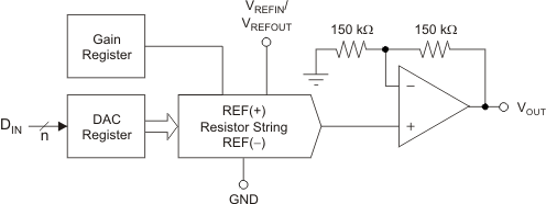 Figure 88. DAC Architecture
The input coding to the DAC756x, DAC816x, and DAC856x devices is straight binary, so the ideal output voltage is given by Equation 1:

where:
n = resolution in bits; either 12 (DAC756x), 14 (DAC816x) or 16 (DAC856x)
DIN = decimal equivalent of the binary code that is loaded to the DAC register. DIN ranges from 0 to 2n – 1.
VREF = DAC reference voltage; either VREFOUT from the internal 2.5-V reference or VREFIN from an
aaa external reference.
Gain = 1 by default when internal reference is disabled (using external reference), and gain = 2 by default
aaa when using internal reference. Gain can also be manually set to either 1 or 2 using the gain register.
aaa See the Gain Function section for more information.
8.3.1.1 Resistor String
The resistor string section is shown in Figure 89. It is simply a string of resistors, each of value R. The code loaded into the DAC register determines at which node on the string the voltage is tapped off to be fed into the output amplifier by closing one of the switches connecting the string to the amplifier. The resistor string architecture results in monotonicity. The RDIVIDER switch is controlled by the gain registers (see the Gain Function section). Because the output amplifier has a gain of 2, RDIVIDER is not shorted when the DAC-n gain is set to 1 (default if internal reference is disabled), and is shorted when the DAC-n gain is set to 2 (default if internal reference is enabled).
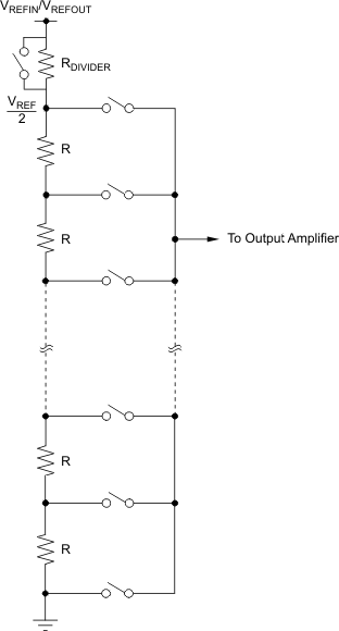 Figure 89. Resistor String
8.3.1.2 Output Amplifier
The output buffer amplifier is capable of generating rail-to-rail voltages on its output, giving a maximum output range of 0 V to AVDD. It is capable of driving a load of 2 kΩ in parallel with 3 nF to GND. The typical slew rate is 0.75 V/µs, with a typical full-scale settling time of 14 µs as shown in Figure 31, Figure 32, Figure 75 and Figure 76.
8.3.2 Internal Reference
The DAC756x, DAC816x, and DAC856x devices include a 2.5-V internal reference that is disabled by default. The internal reference is externally available at the VREFIN/VREFOUT pin. The internal reference output voltage is 2.5 V and can sink and source up to 20 mA.
A minimum 150-nF capacitor is recommended between the reference output and GND for noise filtering.
The internal reference of the DAC756x, DAC816x, and DAC856x devices is a bipolar transistor-based precision band-gap voltage reference. Figure 90 shows the basic band-gap topology. Transistors Q1 and Q2 are biased such that the current density of Q1 is greater than that of Q2. The difference of the two base-emitter voltages (VBE1 – VBE2) has a positive temperature coefficient and is forced across resistor R1. This voltage is amplified and added to the base-emitter voltage of Q2, which has a negative temperature coefficient. The resulting output voltage is virtually independent of temperature. The short-circuit current is limited by design to approximately 100 mA.
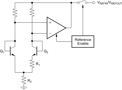 Figure 90. Band-Gap Reference Simplified Schematic
8.3.3 Power-On Reset
8.3.3.1 Power-On Reset to Zero-Scale
The DAC7562, DAC8162, and DAC8562 devices contain a power-on-reset circuit that controls the output voltage during power up. All device registers are reset as shown in Table 4. At power up, all DAC registers are filled with zeros and the output voltages of all DAC channels are set to zero volts. Each DAC channel remains that way until a valid load command is written to it. The power-on reset is useful in applications where it is important to know the state of the output of each DAC while the device is in the process of powering up. No device pin should be brought high before applying power to the device. The internal reference is disabled by default and remains that way until a valid reference-change command is executed.
8.3.3.2 Power-On Reset to Mid-Scale
The DAC7563, DAC8163, and DAC8563 devices contain a power-on reset circuit that controls the output voltage during power up. At power up, all DAC registers are reset to mid-scale code and the output voltages of all DAC channels are set to VREFIN / 2 volts. Each DAC channel remains that way until a valid load command is written to it. The power-on reset is useful in applications where it is important to know the state of the output of each DAC while the device is in the process of powering up. No device pin should be brought high before applying power to the device. The internal reference is powered off or down by default and remains that way until a valid reference-change command is executed. If using an external reference, it is acceptable to power on the VREFIN pin either at the same time as or after applying AVDD.
Table 4. DACxx62 and DACxx63 Power-On Reset Values
| REGISTER | DEFAULT SETTING | |
|---|---|---|
| DAC and input registers | DACxx62 | Zero-scale |
| DACxx63 | Mid-scale | |
| LDAC registers | LDAC pin enabled for both channels | |
| Power-down registers | DACs powered up | |
| Internal reference register | Internal reference disabled | |
| Gain registers | Gain = 1 for both channels | |
8.3.3.3 Power-On Reset (POR) Levels
When the device powers up, a POR circuit sets the device in default mode as shown in Table 4. The POR circuit requires specific AVDD levels, as indicated in Figure 91, to ensure discharging of internal capacitors and to reset the device on power up. In order to ensure a power-on reset, AVDD must be below 0.7 V for at least 1 ms. When AVDD drops below 2.2 V but remains above 0.7 V (shown as the undefined region), the device may or may not reset under all specified temperature and power-supply conditions. In this case, TI recommends a power-on reset. When AVDD remains above 2.2 V, a power-on reset does not occur.
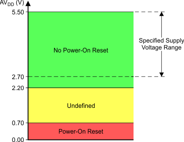 Figure 91. Relevant Voltage Levels for POR Circuit
8.4 Device Functional Modes
8.4.1 Power-Down Modes
The DAC756x, DAC816x, and DAC856x devices have two separate sets of power-down commands. One set is for the DAC channels and the other set is for the internal reference. The internal reference is forced to a powered-down state while both DAC channels are powered down, and is only enabled if any DAC channel is also in the normal mode of operation. For more information on the internal reference control, see the Internal Reference Enable Register section.
8.4.1.1 DAC Power-Down Commands
The DAC756x, DAC816x, and DAC856x DACs use four modes of operation. These modes are accessed by setting the serial interface command bits to 100. Once the command bits are set correctly, the four different power-down modes are software programmable by setting bits DB5 and DB4 in the shift register. Table 5 and Table 6 show the different power-down options. For more information on how to set the DAC operating mode see Table 17.
Table 5. DAC-n Operating Modes
| DB5 | DB4 | DAC Modes of Operation |
|---|---|---|
| 0 | 0 | Selected DACs power up (normal mode, default) |
| 0 | 1 | Selected DACs power down, output 1 kΩ to GND |
| 1 | 0 | Selected DACs power down, output 100 kΩ to GND |
| 1 | 1 | Selected DACs power down, output Hi-Z to GND |
Table 6. DAC-n Selection for Operating Modes
| DAC-B (DB1), DAC-A (DB0) | Operating Mode |
|---|---|
| 0 | DAC-n does not change operating mode |
| 1 | DAC-n operating mode set to value on PD1 and PD0 |
It is possible to write to the DAC register or buffer of the DAC channel that is powered down. When the DAC channel is then powered up, it powers up to this new value.
The advantage of the available power-down modes is that the output impedance of the device is known while it is in power-down mode. As described in Table 5, there are three different power-down options. VOUT can be connected internally to GND through a 1-kΩ resistor, a 100-kΩ resistor, or open-circuited (Hi-Z). The DAC power-down circuitry is shown in Figure 92.
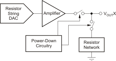 Figure 92. Output Stage
8.4.2 Gain Function
The gain register controls the GAIN setting in the DAC transfer function:

The DAC756x, DAC816x, and DAC856x devices have a gain register for each channel. The gain for each channel, in Equation 2, is either 1 or 2. This gain is automatically set to 2 when using the internal reference, and is automatically set to 1 when the internal reference is disabled (default). However, each channel can have either gain by setting the registers appropriately. The gain registers are accessible by setting the serial interface command bits to 000, address bits to 010, and using DB1 for DAC-B and DB0 for DAC-A. See Table 7 and Table 17 for the full command structure. The gain registers are automatically reset to provide either gain of 1 or 2 when the internal reference is powered off or on, respectively. After the reference is powered off or on, the gain register is again accessible to change the gain.
Table 7. DAC-n Selection for Gain Register Command
| DB1, DB0 | Value | Gain |
|---|---|---|
| DB0 | 0 | DAC-A uses gain = 2 (default with internal reference) |
| 1 | DAC-A uses gain = 1 (default with external reference) | |
| DB1 | 0 | DAC-B uses gain = 2 (default with internal reference) |
| 1 | DAC-B uses gain = 1 (default with external reference) |
8.4.3 Software Reset Function
The DAC756x, DAC816x, and DAC856x devices contain a software reset feature. The software reset function is accessed by setting the serial interface command bits to 101. The software reset command contains two reset modes which are software-programmable by setting bit DB0 in the shift register. Table 8 and Table 17 show the available software reset commands.
Table 8. Software Reset
| DB0 | Registers Reset to Default Values |
|---|---|
| 0 | DAC registers Input registers |
| 1 | DAC registers Input registers LDAC registers Power-down registers Internal reference register Gain registers |
8.4.4 Internal Reference Enable Register
The internal reference in the DAC756x, DAC816x, and DAC856x devices is disabled by default for debugging, evaluation purposes, or when using an external reference. The internal reference can be powered up and powered down by setting the serial interface command bits to 111 and configuring DB0 (see Table 9). The internal reference is forced to a powered down state while both DAC channels are powered down, and can only be enabled if any DAC channel is in normal mode of operation. During the time that the internal reference is disabled, the DAC functions normally using an external reference. At this point, the internal reference is disconnected from the VREFIN/VREFOUT pin (Hi-Z output).
Table 9. Internal Reference
| DB0 | Internal Reference Configuration |
|---|---|
| 0 | Disable internal reference and reset DACs to gain = 1 |
| 1 | Enable internal reference and reset DACs to gain = 2 |
8.4.4.1 Enabling Internal Reference
To enable the internal reference, refer to the command structure in Table 17. When performing a power cycle to reset the device, the internal reference is switched off (default mode). In the default mode, the internal reference is powered down until a valid write sequence powers up the internal reference. However, the internal reference is forced to a disabled state while both DAC channels are powered down, and remains disabled until either DAC channel is returned to the normal mode of operation. See DAC Power-Down Commands for more information on DAC channel modes of operation.
8.4.4.2 Disabling Internal Reference
To disable the internal reference, refer to the command structure in Table 17. When performing a power cycle to reset the device, the internal reference is disabled (default mode).
8.4.5 CLR Functionality
The edge-triggered CLR pin can be used to set the input and DAC registers immediately according to Table 10. When the CLR pin receives a falling edge signal the clear mode is activated and changes the DAC output voltages accordingly. The device exits clear mode on the 24th falling edge of the next write to the device. If the CLR pin receives a falling edge signal during a write sequence in normal operation, the clear mode is activated and changes the input and DAC registers immediately according to Table 10.
Table 10. Clear Mode Reset Values
| DEVICE | DAC Output Entering Clear Mode |
|---|---|
| DAC8562, DAC8162, DAC7562 | Zero-scale |
| DAC8563, DAC8163, DAC7563 | Mid-scale |
8.4.6 LDAC Functionality
The DAC756x, DAC816x, and DAC856x devices offer both a software and hardware simultaneous update and control function. The DAC double-buffered architecture has been designed so that new data can be entered for each DAC without disturbing the analog outputs.
DAC756x, DAC816x, and DAC856x data updates can be performed either in synchronous or in asynchronous mode.
In asynchronous mode, the LDAC pin is used as a negative edge-triggered timing signal for simultaneous DAC updates. Multiple single-channel writes can be done in order to set different channel buffers to desired values and then make a falling edge on LDAC pin to simultaneously update the DAC output registers. Data buffers of all channels must be loaded with desired data before an LDAC falling edge. After a high-to-low LDAC transition, all DACs are simultaneously updated with the last contents of the corresponding data buffers. If the content of a data buffer is not changed, the corresponding DAC output remains unchanged after the LDAC pin is triggered. LDAC must be returned high before the next serial command is initiated.
In synchronous mode, data are updated with the falling edge of the 24th SCLK cycle, which follows a falling edge of SYNC. For such synchronous updates, the LDAC pin is not required, and it must be connected to GND permanently or asserted and held low before sending commands to the device.
Alternatively, all DAC outputs can be updated simultaneously using the built-in software function of LDAC. The LDAC register offers additional flexibility and control by allowing the selection of which DAC channel(s) should be updated simultaneously when the LDAC pin is being brought low. The LDAC register is loaded with a 2-bit word (DB1 and DB0) using command bits C2, C1, and C0 (see Table 17). The default value for each bit, and therefore for each DAC channel, is zero. If the LDAC register bit is set to 1, it overrides the LDAC pin (the LDAC pin is internally tied low for that particular DAC channel) and this DAC channel updates synchronously after the falling edge of the 24th SCLK cycle. However, if the LDAC register bit is set to 0, the DAC channel is controlled by the LDAC pin.
The combination of software and hardware simultaneous update functions is particularly useful in applications when updating a DAC channel, while keeping the other channel unaffected; see Table 11 and Table 17 for more information.
Table 11. DAC-n Selection for LDAC Register Command
| DB1, DB0 | Value | LDAC Pin Functionality |
|---|---|---|
| DB0 | 0 | DAC-A uses LDAC pin |
| 1 | DAC-A operates in synchronous mode | |
| DB1 | 0 | DAC-B uses LDAC pin |
| 1 | DAC-B operates in synchronous mode |
8.5 Programming
The DAC756x, DAC816x, and DAC856x devices have a three-wire serial interface (SYNC, SCLK, and DIN; see the table) compatible with SPI, QSPI, and Microwire interface standards, as well as most DSPs. See the Serial Write Operation timing diagram (Figure 1) for an example of a typical write sequence.
The DAC756x, DAC816x, or DAC856x input shift register is 24 bits wide, consisting of two don’t care bits (DB23 to DB22), three command bits (DB21 to DB19), three address bits (DB18 to DB16), and 16 data bits (DB15 to DB0). All 24 bits of data are loaded into the DAC under the control of the serial clock input, SCLK. DB23 (MSB) is the first bit that is loaded into the DAC shift register. DB23 is followed by the rest of the 24-bit word pattern, left-aligned. This configuration means that the first 24 bits of data are latched into the shift register, and any further clocking of data is ignored.
The write sequence begins by bringing the SYNC line low. Data from the DIN line are clocked into the 24-bit shift register on each falling edge of SCLK. The serial clock frequency can be as high as 50 MHz, making the DAC756x, DAC816x, and DAC856x devices compatible with high-speed DSPs. On the 24th falling edge of the serial clock, the last data bit is clocked into the shift register and the shift register locks. Further clocking does not change the shift register data.
After receiving the 24th falling clock edge, the DAC756x, DAC816x, and DAC856x devices decode the three command bits, three address bits and 16 data bits to perform the required function, without waiting for a SYNC rising edge. After the 24th falling edge of SCLK is received, the SYNC line may be kept low or brought high. In either case, the minimum delay time from the 24th falling SCLK edge to the next falling SYNC edge must be met in order to begin the next cycle properly; see the Serial Write Operation timing diagram (Figure 1).
A rising edge of SYNC before the 24-bit sequence is complete resets the SPI interface; no data transfer occurs. A new write sequence starts at the next falling edge of SYNC. To assure the lowest power consumption of the device, care should be taken that the levels are as close to each rail as possible.
8.5.1 SYNC Interrupt
In a normal write sequence, the SYNC line stays low for at least 24 falling edges of SCLK and the addressed DAC register updates on the 24th falling edge. However, if SYNC is brought high before the 23rd falling edge, it acts as an interrupt to the write sequence; the shift register resets and the write sequence is discarded. Neither an update of the data buffer contents, DAC register contents, nor a change in the operating mode occurs (as shown in Figure 93).
 Figure 93. SYNC Interrupt Facility
8.5.2 DAC Register Configuration
When the DAC registers are being written to, the DAC756x, DAC816x, and DAC856x devices receive all 24 bits of data, ignore DB23 and DB22, and decode the next three bits (DB21 to DB19) in order to determine the DAC operating or control mode (see Table 12). Bits DB18 to DB16 are used to address the DAC channels (see Table 13).
Table 12. Commands for the DAC756x, DAC816x, and DAC856x Devices
| C2 (DB21) |
C1 (DB20) |
C0 (DB19) |
Command |
|---|---|---|---|
| 0 | 0 | 0 | Write to input register n (Table 13) |
| 0 | 0 | 1 | Software LDAC, update DAC register n (Table 13) |
| 0 | 1 | 0 | Write to input register n (Table 13) and update all DAC registers |
| 0 | 1 | 1 | Write to input register n and update DAC register n (Table 13) |
| 1 | 0 | 0 | Set DAC power up or -down mode |
| 1 | 0 | 1 | Software reset |
| 1 | 1 | 0 | Set LDAC registers |
| 1 | 1 | 1 | Enable or disable the internal reference |
Table 13. Address Select for the DAC756x, DAC816x, and DAC856x Devices
| A2 (DB18) |
A1 (DB17) |
A0 (DB16) |
Channel (n) |
|---|---|---|---|
| 0 | 0 | 0 | DAC-A |
| 0 | 0 | 1 | DAC-B |
| 0 | 1 | 0 | Gain (only use with command 000) |
| 0 | 1 | 1 | Reserved |
| 1 | 0 | 0 | Reserved |
| 1 | 0 | 1 | Reserved |
| 1 | 1 | 0 | Reserved |
| 1 | 1 | 1 | DAC-A and DAC-B |
When writing to the DAC input registers the next 16, 14, or 12 bits of data that follow are decoded by the DAC to determine the equivalent analog output (see Table 14 through Table 16) . The data format is straight binary, with all 0s corresponding to 0-V output and all 1s corresponding to full-scale output. For all documentation purposes, the data format and representation used here is a true 16-bit pattern (that is, FFFFh data word for full scale) that the DAC756x, DAC816x, and DAC856x devices require.
Table 14. DAC856x Data Input Register Format
| COMMAND | ADDRESS | DATA | ||||||||||||||||||||||
|---|---|---|---|---|---|---|---|---|---|---|---|---|---|---|---|---|---|---|---|---|---|---|---|---|
| X(1) | X | C2 | C1 | C0 | A2 | A1 | A0 | D15 | D14 | D13 | D12 | D11 | D10 | D9 | D8 | D7 | D6 | D5 | D4 | D3 | D2 | D1 | D0 | |
| DB23 | DB0 | |||||||||||||||||||||||
Table 15. DAC816x Data Input Register Format
| COMMAND | ADDRESS | DATA | ||||||||||||||||||||||
|---|---|---|---|---|---|---|---|---|---|---|---|---|---|---|---|---|---|---|---|---|---|---|---|---|
| X | X | C2 | C1 | C0 | A2 | A1 | A0 | D13 | D12 | D11 | D10 | D9 | D8 | D7 | D6 | D5 | D4 | D3 | D2 | D1 | D0 | X | X | |
| DB23 | DB0 | |||||||||||||||||||||||
Table 16. DAC756x Data Input Register Format
| COMMAND | ADDRESS | DATA | ||||||||||||||||||||||
|---|---|---|---|---|---|---|---|---|---|---|---|---|---|---|---|---|---|---|---|---|---|---|---|---|
| X | X | C2 | C1 | C0 | A2 | A1 | A0 | D11 | D10 | D9 | D8 | D7 | D6 | D5 | D4 | D3 | D2 | D1 | D0 | X | X | X | X | |
| DB23 | DB0 | |||||||||||||||||||||||
In additon to DAC input register updates, the DAC756x, DAC816x, and DAC856x devices support a number of functional mode commands (such as write to LDAC register, power down DACs and so on). The complete set of functional mode commands is shown in Table 17.
Table 17. Command Matrix for the DAC756x, DAC816x, and DAC856x Devices
| DB23-DB22 | Command | Address | Data | DESCRIPTION | |||||||||
|---|---|---|---|---|---|---|---|---|---|---|---|---|---|
| C2 | C1 | C0 | A2 | A1 | A0 | DB15-DB6 | DB5 | DB4 | DB3-DB2 | DB1 | DB0 | ||
| X(1) | 0 | 0 | 0 | 0 | 0 | 0 | 16-, 14-, or 12-bit DAC data | Write to DAC-A input register | |||||
| 0 | 0 | 1 | 16-, 14-, or 12-bit DAC data | Write to DAC-B input register | |||||||||
| 1 | 1 | 1 | 16-, 14-, or 12-bit DAC data | Write to DAC-A and DAC-B input registers | |||||||||
| X | 0 | 1 | 0 | 0 | 0 | 0 | 16-, 14-, or 12-bit DAC data | Write to DAC-A input register and update all DACs | |||||
| 0 | 0 | 1 | 16-, 14-, or 12-bit DAC data | Write to DAC-B input register and update all DACs | |||||||||
| 1 | 1 | 1 | 16-, 14-, or 12-bit DAC data | Write to DAC-A and DAC-B input register and update all DACs | |||||||||
| X | 0 | 1 | 1 | 0 | 0 | 0 | 16-, 14-, or 12-bit DAC data | Write to DAC-A input register and update DAC-A | |||||
| 0 | 0 | 1 | 16-, 14-, or 12-bit DAC data | Write to DAC-B input register and update DAC-B | |||||||||
| 1 | 1 | 1 | 16-, 14-, or 12-bit DAC data | Write to DAC-A and DAC-B input register and update all DACs | |||||||||
| X | 0 | 0 | 1 | 0 | 0 | 0 | X | Update DAC-A | |||||
| 0 | 0 | 1 | X | Update DAC-B | |||||||||
| 1 | 1 | 1 | X | Update all DACs | |||||||||
| X | 0 | 0 | 0 | 0 | 1 | 0 | X | 0 | 0 | Gain: DAC-B gain = 2, DAC-A gain = 2 (default with internal VREF) | |||
| 0 | 1 | Gain: DAC-B gain = 2, DAC-A gain = 1 | |||||||||||
| 1 | 0 | Gain: DAC-B gain = 1, DAC-A gain = 2 | |||||||||||
| 1 | 1 | Gain: DAC-B gain = 1, DAC-A gain = 1 (power-on default) | |||||||||||
| X | 1 | 0 | 0 | X | X | 0 | 0 | X | 0 | 1 | Power up DAC-A | ||
| 1 | 0 | Power up DAC-B | |||||||||||
| 1 | 1 | Power up DAC-A and DAC-B | |||||||||||
| X | 1 | 0 | 0 | X | X | 0 | 1 | X | 0 | 1 | Power down DAC-A; 1 kΩ to GND | ||
| 1 | 0 | Power down DAC-B; 1 kΩ to GND | |||||||||||
| 1 | 1 | Power down DAC-A and DAC-B; 1 kΩ to GND | |||||||||||
| X | 1 | 0 | 0 | X | X | 1 | 0 | X | 0 | 1 | Power down DAC-A; 100 kΩ to GND | ||
| 1 | 0 | Power down DAC-B; 100 kΩ to GND | |||||||||||
| 1 | 1 | Power down DAC-A and DAC-B; 100 kΩ to GND | |||||||||||
| X | 1 | 0 | 0 | X | X | 1 | 1 | X | 0 | 1 | Power down DAC-A; Hi-Z | ||
| 1 | 0 | Power down DAC-B; Hi-Z | |||||||||||
| 1 | 1 | Power down DAC-A and DAC-B; Hi-Z | |||||||||||
| X | 1 | 0 | 1 | X | X | X | 0 | Reset DAC-A and DAC-B input register and update all DACs | |||||
| X | 1 | Reset all registers and update all DACs (Power-on-reset update) | |||||||||||
| X | 1 | 1 | 0 | X | X | 0 | 0 | LDAC pin active for DAC-B and DAC-A | |||||
| 0 | 1 | LDAC pin active for DAC-B; inactive for DAC-A | |||||||||||
| 1 | 0 | LDAC pin inactive for DAC-B; active for DAC-A | |||||||||||
| 1 | 1 | LDAC pin inactive for DAC-B and DAC-A | |||||||||||
| X | 1 | 1 | 1 | X | X | X | 0 | Disable internal reference and reset DACs to gain = 1 | |||||
| X | 1 | Enable internal reference and reset DACs to gain = 2 | |||||||||||