SBAS538D December   2013  – December 2021 DAC7750 , DAC8750

PRODUCTION DATA  

  1. Features
  2. Applications
  3. Description
  4. Revision History
  5. Device Comparison Table
  6. Pin Configuration and Functions
  7. Specifications
    1. 7.1  Absolute Maximum Ratings
    2. 7.2  ESD Ratings
    3. 7.3  Recommended Operating Conditions
    4. 7.4  Thermal Information
    5. 7.5  Electrical Characteristics
    6. 7.6  Electrical Characteristics: AC
    7. 7.7  Timing Requirements: Write Mode
    8. 7.8  Timing Requirements: Readback Mode
    9. 7.9  Timing Diagrams
    10. 7.10 Typical Characteristics
  8. Detailed Description
    1. 8.1 Overview
    2. 8.2 Functional Block Diagram
    3. 8.3 Feature Description
      1. 8.3.1  DAC Architecture
      2. 8.3.2  Current Output Stage
      3. 8.3.3  Internal Reference
      4. 8.3.4  Digital Power Supply
      5. 8.3.5  DAC Clear
      6. 8.3.6  Power-On Reset
      7. 8.3.7  Alarm Detection
      8. 8.3.8  Watchdog Timer
      9. 8.3.9  Frame Error Checking
      10. 8.3.10 User Calibration
      11. 8.3.11 Programmable Slew Rate
    4. 8.4 Device Functional Modes
      1. 8.4.1 Setting Current-Output Ranges
      2. 8.4.2 Current-Setting Resistor
      3. 8.4.3 BOOST Configuration for IOUT
      4. 8.4.4 Filtering The Current Output
      5. 8.4.5 Output Current Monitoring
      6. 8.4.6 HART Interface
        1. 8.4.6.1 Implementing HART in 4-mA to 20-mA Mode
        2. 8.4.6.2 Implementing HART in All Current Output Modes
    5. 8.5 Programming
      1. 8.5.1 Serial Peripheral Interface (SPI)
        1. 8.5.1.1 SPI Shift Register
        2. 8.5.1.2 Write Operation
        3. 8.5.1.3 Read Operation
        4. 8.5.1.4 Stand-Alone Operation
        5. 8.5.1.5 Multiple Devices on the Bus
    6. 8.6 Register Maps
      1. 8.6.1 DACx750 Register Descriptions
        1. 8.6.1.1 Control Register
        2. 8.6.1.2 Configuration Register
        3. 8.6.1.3 DAC Registers
        4. 8.6.1.4 Reset Register
        5. 8.6.1.5 Status Register
  9. Application and Implementation
    1. 9.1 Application Information
      1. 9.1.1 HART Implementation
        1. 9.1.1.1 Using the CAP2 Pin
        2. 9.1.1.2 Using the ISET-R Pin
    2. 9.2 Typical Application
      1. 9.2.1 Design Requirements
      2. 9.2.2 Detailed Design Procedure
      3. 9.2.3 Application Curve
  10. 10Power Supply Recommendations
  11. 11Layout
    1. 11.1 Layout Guidelines
      1. 11.1.1 Thermal Considerations
    2. 11.2 Layout Example
  12. 12Device and Documentation Support
    1. 12.1 Documentation Support
      1. 12.1.1 Related Documentation
    2. 12.2 Receiving Notification of Documentation Updates
    3. 12.3 Support Resources
    4. 12.4 Trademarks
    5. 12.5 Electrostatic Discharge Caution
    6. 12.6 Glossary
  13. 13Mechanical, Packaging, and Orderable Information

Package Options

Mechanical Data (Package|Pins)
Thermal pad, mechanical data (Package|Pins)
Orderable Information

Typical Characteristics

at TA = 25°C (unless otherwise noted)
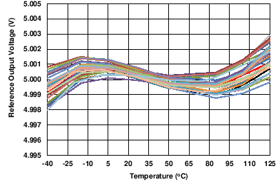
GUID-2B85A96C-FD1D-4A2F-9A34-3F95AF1791E6-low.png
30 units shownAVDD = 24 V
Figure 7-3 REFOUT vs Temperature
GUID-3AD25EE8-2089-45B2-90A9-003C11B32370-low.png
AVDD = 24 V
Figure 7-5 REFOUT vs Load Current
GUID-4E83B5F1-565A-4729-A351-18D006776870-low.png
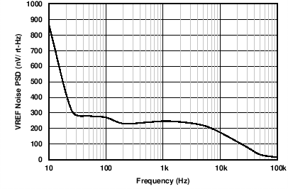
AVDD = 24 V
Figure 7-7 REFOUT Noise PSD vs Frequency
GUID-63F9CC1C-7F58-4D16-BFA5-0E3587639D29-low.png
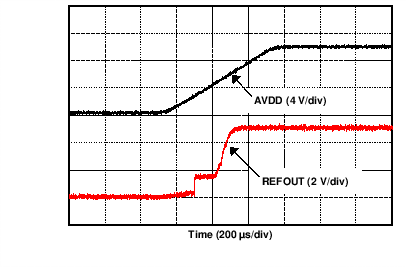
AVDD = 10 V
Figure 7-9 REFOUT Transient vs Time
GUID-E3E69907-2CBC-4BE6-A3D9-32F109960A63-low.png
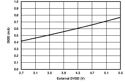
TA = 25°CExternal DVDD
Figure 7-11 DIDD vs External DVDD
GUID-DA16D61B-B5D9-4ED8-A9E7-8DCDB023D432-low.png
AVDD = 18 VCLOAD = 100 nF
Figure 7-13 Internal DVDD PSRR vs Frequency
GUID-DBB48AAD-6537-457B-AD61-15174C02D7C1-low.png
AVDD = 24 VRLOAD = 300 Ω
Figure 7-15 IOUT TUE vs Code (0 mA to 20 mA)
GUID-8217EE9C-BC84-475C-A005-E9F3F3741AB5-low.png
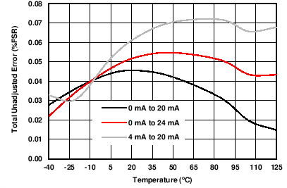
AVDD = 10 VRLOAD = 300 Ω
Figure 7-17 IOUT TUE vs Temperature (Internal RSET)
GUID-82ACD91B-A48A-44D0-B3A3-5A42EAB8F65F-low.png
RLOAD = 300 Ω0-mA to 24-mA range
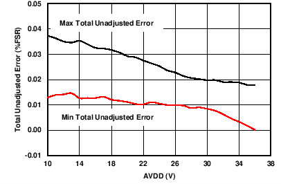
Figure 7-19 IOUT TUE vs Supply (Internal RSET)
GUID-F446F9E9-4FC7-440D-A00E-DB1980E21522-low.png
AVDD = 24 VRLOAD = 300 Ω
Figure 7-21 IOUT INL vs Code (0 mA to 24 mA)
GUID-2C9619C6-4F2D-4C35-B83C-CA8C23A5C044-low.png
AVDD = 24 VRLOAD = 300 Ω
Figure 7-23 IOUT INL vs Code (4 mA to 20 mA)
GUID-469C30E9-8A28-4082-829B-BB2DBA695197-low.png
AVDD = 10 VRLOAD = 300 ΩAll IOUT ranges
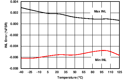
Figure 7-25 IOUT INL vs Temperature (External RSET)
GUID-CF80EE03-B2D4-4512-8C7D-17A64037CE7E-low.png
RLOAD = 300 Ω0-mA to 24-mA range
 
Figure 7-27 IOUT INL vs Supply (External RSET)
GUID-BEA6DA70-2C61-4963-AC2B-25CEE13A5D92-low.png
AVDD = 24 V0-mA to 24-mA range
RLOAD = 300 Ω
Figure 7-29 IOUT DNL vs Code (0 mA to 20 mA)
GUID-39336BB1-2DF6-472D-946D-36E7E4F03925-low.png
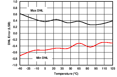
AVDD = 10 VRLOAD = 300 ΩAll IOUT ranges
Figure 7-31 IOUT DNL vs Temperature (Internal RSET)
GUID-3914F321-D75A-45B8-9822-DB12F7D0960B-low.png
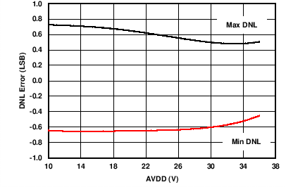
RLOAD = 300 Ω0-mA to 24-mA range
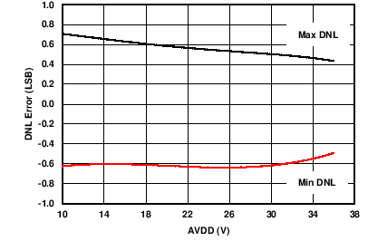
Figure 7-33 IOUT DNL vs Supply (Internal RSET)
GUID-57D25006-D1E0-4085-A0D0-EB0B220DF65C-low.png
AVDD = 10 VRLOAD = 300 Ω
Figure 7-35 IOUT Full-Scale Error vs Temperature
GUID-2833401F-62AB-4F7A-86BB-F33DD1CA21AF-low.png
AVDD = 10 VRLOAD = 300 Ω
Figure 7-37 IOUT Gain Error vs Temperature
GUID-E70620D6-8A3F-4B52-81E9-618E3574091F-low.png
 
 
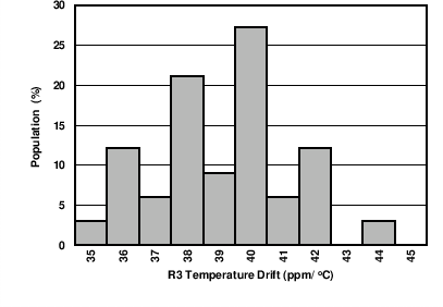
Figure 7-39 R3 Resistance Temperature Drift Histogram
GUID-6798BEF5-5FFC-465B-A42C-251517ECC4F3-low.png
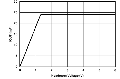
AVDD = 36 V RLOAD = 300 Ω
DAC configured to deliver 24 mA
NOTE: Compliance voltage headroom is defined as the drop from the AVDD pin to the IOUT pin.
Figure 7-41 IOUT vs Compliance Headroom Voltage
GUID-ED8854C5-81F7-43E8-943B-01E338A96F22-low.png
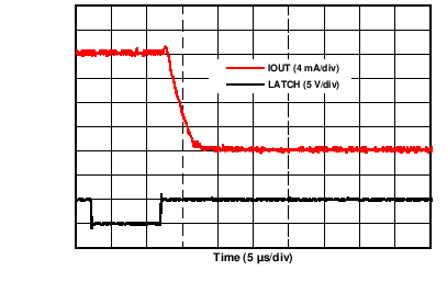
AVDD = 24 V 4-mA to 20-mA range
RLOAD = 300 Ω From code: 0x0000 To code: 0xFFFF
Figure 7-43 4-mA to 20-mA Falling
GUID-72896AD2-279A-4308-B2C1-5B8BA916E09A-low.png
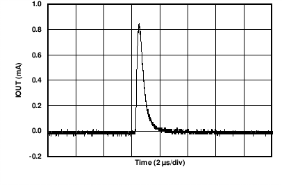
AVDD = 24 VRLOAD = 300 Ω
Figure 7-45 IOUT Output Enable Glitch
GUID-D851B656-0CB4-473D-B1CE-567CD1DC2AD3-low.png
AVDD = 24 VRLOAD = 300 ΩAll IOUT ranges
 
Figure 7-47 IOUT Noise PSD vs Frequency
GUID-2AF5221F-BDFE-4F44-B4EA-D22A90897D35-low.png
AVDD = 36 VOutput disabled
Figure 7-49 IOUT Hi-Z Leakage Current vs Voltage
GUID-981D7E7A-9D1B-49F8-8503-78AC6DB9D3BA-low.pngFigure 7-4 Internal Reference Temperature Drift Histogram
GUID-0E1EB8CA-A99C-4886-AB15-EDD2E8D5DD25-low.png
TA = 25°C
Figure 7-6 REFOUT vs AVDD
GUID-8B0B982F-0679-4409-992C-A6F2D2F14B81-low.png
AVDD = 24 V
Figure 7-8 Internal Reference, Peak-to-Peak Noise (0.1 Hz to 10 Hz)
GUID-32A4D9FA-7C11-4506-A908-9C8A10B15E5A-low.png
External DVDDIOUT = 0 mA
Figure 7-10 AIDD vs AVDD
GUID-012E011C-6780-4BAD-A4A6-B40834BB0159-low.png
TA = 25°C Internal DVDD
Figure 7-12 Internal DVDD vs Load Current
GUID-6267545F-46FA-4473-9FAB-724516CAFD67-low.png
AVDD = 24 VRLOAD = 300 Ω
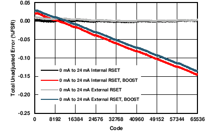
Figure 7-14 IOUT TUE vs Code (0 mA to 24 mA)
GUID-E659FF5B-F9FF-4B7B-B57A-17B59BA84BB7-low.png
AVDD = 24 VRLOAD = 300 Ω
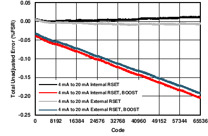
Figure 7-16 IOUT TUE vs Code (4 mA to 20 mA)
GUID-745C313E-1728-4870-808B-89C449F2BCE3-low.png
AVDD = 10 VRLOAD = 300 Ω
Figure 7-18 IOUT TUE vs Temperature (External RSET)
GUID-5F26CF3E-AD38-4776-8C47-5A1AC9B07922-low.png
RLOAD = 300 Ω 0-mA to 24-mA range
Figure 7-20 IOUT TUE vs Supply (External RSET)
GUID-7C6CC9F2-7AFD-439C-AF85-BBAA0EFF8781-low.png
AVDD = 24 VRLOAD = 300 Ω
Figure 7-22 IOUT INL vs Code (0 mA to 20 mA)
GUID-5728FFA4-8203-43CE-AE7C-27474B58A43C-low.png
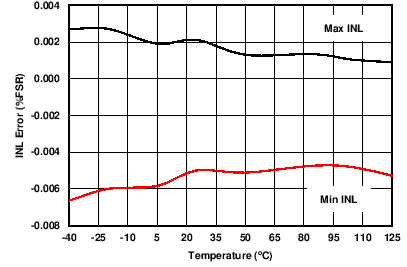
AVDD = 10 VRLOAD = 300 ΩAll IOUT ranges
Figure 7-24 IOUT INL vs Temperature (Internal RSET)
GUID-F7B178C4-E06A-4390-858E-4CB09D7CF1DD-low.png
RLOAD = 300 Ω0-mA to 24-mA range
Figure 7-26 IOUT INL vs Supply (Internal RSET)
GUID-4B4016EB-4B07-480A-A3B8-2E7AE6F244F0-low.png
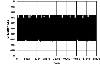
AVDD = 24 V0-mA to 24-mA range
RLOAD = 300 Ω
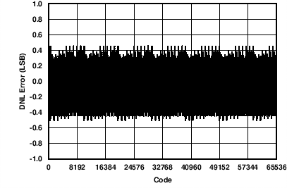
Figure 7-28 IOUT DNL vs Code (0 mA to 24 mA)
GUID-C05ECDAF-2012-457D-82E8-D0F6682FDAAC-low.png
AVDD = 24 V4-mA to 24-mA range
RLOAD = 300 Ω
Figure 7-30 IOUT DNL vs Code (4 mA to 20 mA)
GUID-D60229A8-FBAC-4CFA-8A3B-A9880E7BFC1C-low.png
AVDD = 10 VRLOAD = 300 ΩAll IOUT ranges
Figure 7-32 IOUT DNL vs Temperature (External RSET)
GUID-7944B4E9-C864-46D1-999C-C34ECEA82568-low.png
RLOAD = 300 Ω0-mA to 24-mA range
Figure 7-34 IOUT DNL vs Supply (External RSET)
GUID-A5DA2AF6-0672-4837-B015-844D6AC5CBB1-low.png
AVDD = 10 VRLOAD = 300 Ω
Figure 7-36 IOUT Offset Error vs Temperature
GUID-A13F5D97-0207-4181-AAA2-BECEB114FEA5-low.png
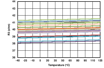
33 units shown
Figure 7-38 R3 Resistance vs Temperature
GUID-F82FF972-70C6-4B5E-8FEB-963108986E39-low.png
AVDD = 36 V IOUT = 24 mA RLOAD = 300 Ω
NOTE: Compliance voltage headroom is defined as the drop from the AVDD pin to the IOUT pin.
Figure 7-40 Compliance Headroom Voltage vs Temperature
GUID-0040A11C-5356-4CB2-89AF-4EB1D6AFA418-low.png
AVDD = 24 V 4-mA to 20-mA range
RLOAD = 300 Ω From code: 0x0000 To code: 0xFFFF
 
 
Figure 7-42 4-mA to 20-mA Rising
GUID-C2ECBD0C-4DD1-488F-BAD0-8A872FA0810A-low.png
AVDD = 24 V RLOAD = 300 Ω
 
Figure 7-44 IOUT Power-On Glitch
GUID-E69D15DF-B603-46C4-9B45-E4B545382CC3-low.png
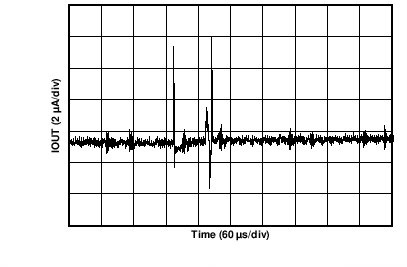
AVDD = 24 VRLOAD = 250 Ω
Figure 7-46 IOUT Digital-to-Analog Glitch
GUID-F2464BEF-47AC-4D9E-ABE2-A420998AB009-low.png
AVDD = 24 V0-mA to 20-mA range
DAC = midscale
Figure 7-48 IOUT Peak-to-Peak Noise vs Time (0.1 Hz to 10 Hz)
GUID-68EF7175-8FD8-47EF-A633-BB99D63B7142-low.png
AVDD = 24 VRLOAD = 250 ΩAll IOUT ranges
Figure 7-50 IOUT PSRR vs Frequency