SBAS793A November   2019  – April 2020 DAC60502 , DAC70502 , DAC80502

PRODUCTION DATA.  

  1. Features
  2. Applications
  3. Description
    1.     Device Images
      1.      Functional Block Diagram
  4. Revision History
  5. Device Comparison Table
  6. Pin Configuration and Functions
    1.     Pin Functions
  7. Specifications
    1. 7.1  Absolute Maximum Ratings
    2. 7.2  ESD Ratings
    3. 7.3  Recommended Operating Conditions
    4. 7.4  Thermal Information
    5. 7.5  Electrical Characteristics
    6. 7.6  Timing Requirements : SPI Mode
    7. 7.7  Timing Requirements : I2C Standard Mode
    8. 7.8  Timing Requirements : I2C Fast Mode
    9. 7.9  Timing Requirements : I2C Fast-Mode Plus
    10. 7.10 Typical Characteristics
  8. Detailed Description
    1. 8.1 Overview
    2. 8.2 Functional Block Diagram
    3. 8.3 Feature Description
      1. 8.3.1 Digital-to-Analog Converter (DAC) Architecture
        1. 8.3.1.1 DAC Transfer Function
        2. 8.3.1.2 DAC Register Structure
        3. 8.3.1.3 Output Amplifier
      2. 8.3.2 Internal Reference
        1. 8.3.2.1 Solder Heat Reflow
      3. 8.3.3 Power-On Reset (POR)
      4. 8.3.4 Software Reset
    4. 8.4 Device Functional Modes
      1. 8.4.1 Power-Down Mode
    5. 8.5 Programming
      1. 8.5.1 Serial Interface
        1. 8.5.1.1 SPI Mode
          1. 8.5.1.1.1 SYNC Interrupt
        2. 8.5.1.2 I2C Mode
          1. 8.5.1.2.1 F/S Mode Protocol
          2. 8.5.1.2.2 DACx0502 I2C Update Sequence
            1. 8.5.1.2.2.1 DACx0502 Address Byte
            2. 8.5.1.2.2.2 DACx0502 Command Byte
            3. 8.5.1.2.2.3 DACx0502 Data Byte (MSDB and LSDB)
          3. 8.5.1.2.3 DACx0502 I2C Read Sequence
    6. 8.6 Register Maps
      1. 8.6.1 Registers
        1. 8.6.1.1 NOOP Register (offset = 0h) [reset = 0000h]
          1. Table 9. NOOP Register Field Descriptions
        2. 8.6.1.2 DEVID Register (offset = 1h) [reset = 0214h for DAC80502, 1214h for DAC70502, 2214h for DAC60502]
          1. Table 10. DEVID Register Field Descriptions
        3. 8.6.1.3 SYNC Register (offset = 2h) [reset = 0300h]
          1. Table 11. SYNC Register Field Descriptions
        4. 8.6.1.4 CONFIG Register (offset = 3h) [reset = 0000h]
          1. Table 12. CONFIG Register Field Descriptions
        5. 8.6.1.5 GAIN Register (offset = 4h) [reset = 0003h]
          1. Table 13. GAIN Register Field Descriptions
        6. 8.6.1.6 TRIGGER Register (offset = 5h) [reset = 0000h]
          1. Table 14. TRIGGER Register Field Descriptions
        7. 8.6.1.7 BRDCAST Register (offset = 6h) [reset = 0000h for RSTSEL = 0, or reset = 8000h for RSTSEL = 1]
          1. Table 15. BRDCAST Register Field Descriptions
        8. 8.6.1.8 STATUS Register (offset = 7h) [reset = 0000h]
          1. Table 16. STATUS Register Field Descriptions
        9. 8.6.1.9 DAC-n Register (offset = 8h–9h) [reset = 0000h for RSTSEL = 0, or reset = 8000h for RSTSEL = 1]
          1. Table 17. DAC-A Data Register Field Descriptions (8h)
          2. Table 18. DAC-B Data Register Field Descriptions (9h)
  9. Application and Implementation
    1. 9.1 Application Information
    2. 9.2 Typical Application
      1. 9.2.1 Design Requirements
      2. 9.2.2 Detailed Design Procedure
      3. 9.2.3 Application Curves
    3. 9.3 System Examples
      1. 9.3.1 SPI Connection to a Processor
      2. 9.3.2 I2C Interface Connection to a Processor
    4. 9.4 What To Do and What Not To Do
      1. 9.4.1 What To Do
      2. 9.4.2 What Not To Do
    5. 9.5 Initialization Setup
  10. 10Power Supply Recommendations
  11. 11Layout
    1. 11.1 Layout Guidelines
    2. 11.2 Layout Example
  12. 12Device and Documentation Support
    1. 12.1 Documentation Support
      1. 12.1.1 Related Documentation
    2. 12.2 Related Links
    3. 12.3 Receiving Notification of Documentation Updates
    4. 12.4 Support Resources
    5. 12.5 Trademarks
    6. 12.6 Electrostatic Discharge Caution
    7. 12.7 Glossary
  13. 13Mechanical, Packaging, and Orderable Information

Package Options

Mechanical Data (Package|Pins)
Thermal pad, mechanical data (Package|Pins)
Orderable Information

I2C Interface Connection to a Processor

The I2C interface on DACx0502 provides a slave address selection pin A0 in addition to the standard SCL and SDA signals. The A0 can be configured to provide four slave addresses, as specified in Table 3. Pull up the SCL and SDA pins, as shown in Figure 76. The pullup resistor must be selected considering the parasitic capacitance of the I2C bus on the printed circuit board (PCB). A small resistance provides better speed, but at the cost of increased power consumption.
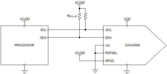
DAC80502 DAC70502 DAC60502 dac80502-i2c-interface-to-processor.gifFigure 76. I2C Interface Connection to a Processor