SLASF62 June 2024 DAC80516
ADVANCE INFORMATION
- 1
- 1 Features
- 2 Applications
- 3 Description
- 4 Pin Configuration and Functions
-
5 Specifications
- 5.1 Absolute Maximum Ratings
- 5.2 ESD Ratings
- 5.3 Recommended Operating Conditions
- 5.4 Thermal Information
- 5.5 Electrical Characteristics
- 5.6 Timing Requirements - I2C Standard Mode
- 5.7 Timing Requirements - I2C Fast Mode
- 5.8 Timing Requirements - I2C Fast Mode Plus
- 5.9 Timing Requirements - SPI
- 5.10 Switching Characteristics
- 5.11 Timing Diagrams
- 5.12 Typical Characteristics
- 6 Detailed Description
- 7 Register Map
- 8 Application and Implementation
- 9 Device and Documentation Support
- 10Revision History
- 11Mechanical, Packaging, and Orderable Information
Package Options
Refer to the PDF data sheet for device specific package drawings
Mechanical Data (Package|Pins)
- RUY|28
Thermal pad, mechanical data (Package|Pins)
Orderable Information
11.1 Tape and Reel Information
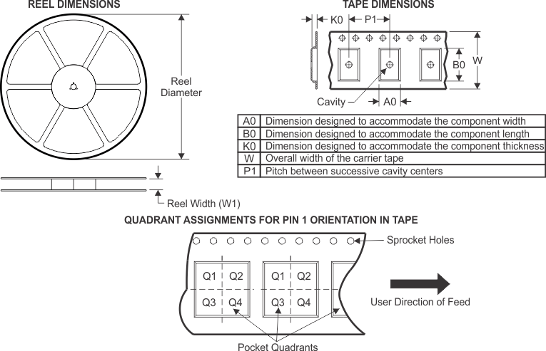
| Device | Package Type |
Package Drawing | Pins | SPQ | Reel Diameter (mm) |
Reel Width W1 (mm) |
A0 (mm) |
B0 (mm) |
K0 (mm) |
P1 (mm) |
W (mm) |
Pin 1 Quadrant |
|---|---|---|---|---|---|---|---|---|---|---|---|---|
| PDAC80516RUYT | WQFN | RUY | 28 | 250 | 330 | 12.4 | 4.25 | 4.25 | 1.15 | 8 | 12 | 2 |
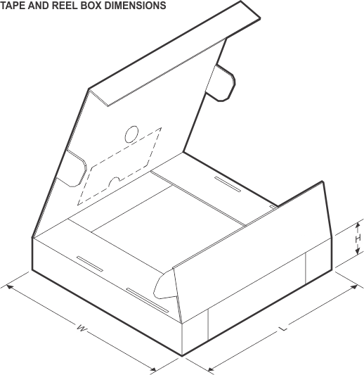
| Device | Package Type | Package Drawing | Pins | SPQ | Length (mm) | Width (mm) | Height (mm) |
|---|---|---|---|---|---|---|---|
| PDAC80516RUYT | WQFN | RUY | 28 | 250 | 367 | 367 | 35 |


