at TJ = 25°C,
AVDD = 5.5V, VIO = 5.5V, internal reference = 2.5V, gain =
2, DAC outputs unloaded (unless otherwise noted)
 Figure 5-3 Integral Nonlinearity vs Digital Input Code
 Figure 5-5 Total Unadjusted Error vs Digital Input Code
 Figure 5-7 Differential Nonlinearity vs Temperature
 Figure 5-9 Offset Error vs Temperature
 Figure 5-11 Gain Error vs Temperature
 Figure 5-13 Integral Nonlinearity vs Supply Voltage
 Figure 5-15 Total Unadjusted Error vs Supply Voltage
 Figure 5-17 Zero-Scale Error vs Supply Voltage
 Figure 5-19 Full-Scale Error vs Supply Voltage
 Figure 5-21 Supply Current With Internal Reference vs Digital Input Code
 Figure 5-23 Supply Current With Internal Reference vs Temperature
 Figure 5-25 Supply Current With Internal Reference vs Supply Voltage
 Figure 5-27 Power-Down Current vs Supply Voltage
 Figure 5-29 Headroom vs Load Current
 Figure 5-31 Source and Sink Capability
 Figure 5-33 Full-Scale Settling Time,
Rising Edge
 Figure 5-35 Glitch Impulse, Falling Edge
 Figure 5-37 Power-On, Reset to Zero Scale
 Figure 5-39 AVDD Power Down Response
 Figure 5-41 Channel-to-Channel DC Crosstalk
| DAC at full-scale, AVDD = 5V +
200mVPP |
|
Figure 5-43 DAC Output AC PSRR vs
Frequency
| DAC at
midscale, gain = 2, external reference = 2.5V |
Figure 5-45 DAC
Output Noise With External Reference 0.1Hz to 10Hz Figure 5-47 Internal Reference Voltage vs Temperature
 Figure 5-49 Internal Reference Voltage vs Internal Reference
Current
 Figure 5-51 Internal Reference Noise
 Figure 5-4 Differential Nonlinearity vs Digital Input Code
 Figure 5-6 Integral Nonlinearity vs Temperature
 Figure 5-8 Total Unadjusted Error vs Temperature
 Figure 5-10 Zero-Scale Error vs Temperature
 Figure 5-12 Full-Scale Error vs Temperature
 Figure 5-14 Differential Nonlinearity vs Supply Voltage
 Figure 5-16 Offset Error vs Supply Voltage
 Figure 5-18 Gain Error vs Supply Voltage
| External reference = 2.5V (gain = 2) |
|
Figure 5-20 Supply Current With External Reference vs Digital Input Code
| External reference = 2.5V (gain = 2) |
|
Figure 5-22 Supply Current With External Reference vs Temperature
| External reference = 2.5V (gain = 1) |
|
Figure 5-24 Supply Current With External Reference vs Supply Voltage Figure 5-26 Power-Down Current vs Temperature
 Figure 5-28 Power-Down Current vs VIO
 Figure 5-30 Headroom vs Load Current
 Figure 5-32 Source and Sink Capability
 Figure 5-34 Full-Scale Settling Time,
Falling Edge
 Figure 5-36 Glitch Impulse, Rising Edge
 Figure 5-38 Clear
to Zero Scale
 Figure 5-40 VIO Power Down Response
| DAC at midscale, SCLK = 1MHz |
|
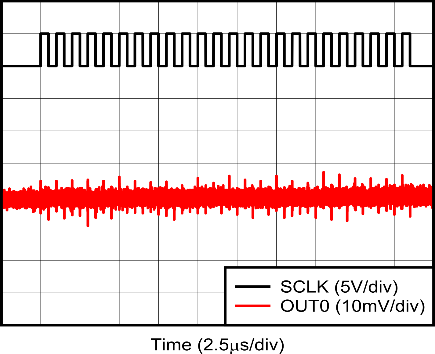
Figure 5-42 Clock
Feedthrough Figure 5-44 DAC
Output Noise Density vs Frequency
 Figure 5-46 DAC
Output Noise With Internal Reference 0.1Hz to 10Hz
 Figure 5-48 Internal Reference Voltage vs Supply Voltage
 Figure 5-50 Internal Reference Noise Density vs Frequency


