-
DACx551-Q1 Automotive 16-, 12-Bit, Ultralow-Glitch, Voltage-Output DAC SLASEB8C February 2016 – November 2016 DAC6551-Q1 , DAC8551-Q1
PRODUCTION DATA.
-
DACx551-Q1 Automotive 16-, 12-Bit, Ultralow-Glitch, Voltage-Output DAC
- 1 Features
- 2 Applications
- 3 Description
- 4 Revision History
- 5 Pin Configuration and Functions
- 6 Specifications
- 7 Detailed Description
- 8 Application and Implementation
- 9 Power Supply Recommendations
- 10Layout
- 11Device and Documentation Support
- 12Mechanical, Packaging, and Orderable Information
- IMPORTANT NOTICE
Package Options
Mechanical Data (Package|Pins)
- DGK|8
Thermal pad, mechanical data (Package|Pins)
Orderable Information
DACx551-Q1 Automotive 16-, 12-Bit, Ultralow-Glitch, Voltage-Output DAC
1 Features
- Qualified for Automotive Applications
- AEC-Q100 Qualified With the Following Results:
- Device Temperature Grade 1: –40°C to 125°C Ambient Operating Temperature Range
- Device HBM ESD Classification Level 2
- Device CDM ESD Classification Level C4B
- Relative Accuracy:
- DAC8551-Q1 (16-Bit): 4 LSB INL
- DAC6551-Q1 (12-Bit): 0.3 LSB INL
- Ultralow Glitch Impulse: 0.1 nV-s
- Settling Time: 8 μs to ±0.003% FSR
- Power Supply: 3 V to 5.5 V
- Power-On Reset to Zero Scale
- MicroPower Operation: 160 μA at 5 V
- Low-Power Serial Interface With Schmitt-Triggered Inputs
- On-Chip Output Buffer Amplifier With Rail-to-Rail Operation
- Power-Down Capability
- Binary Input
- SYNC Interrupt Facility
- Available in a Tiny VSSOP-8 Package
2 Applications
- Automotive Radar
- Automotive Sensors
3 Description
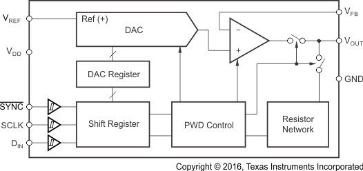
The DAC8551-Q1 and DAC6551-Q1 are small, low-power, voltage-output, 16- and 12-bit digital-to-analog converters (DACs) qualified for automotive applications. The DACx551-Q1 devices provide good linearity and minimize undesired code-to-code transient voltages. The devices use a versatile 3-wire serial interface that operates at clock rates to 30 MHz and is compatible with standard SPI, QSPI, Microwire, and digital signal-processor (DSP) interfaces.
The DACx551-Q1 devices require an external reference voltage to set the output range. The devices incorporate a power-on-reset circuit that ensures the DAC output powers up at 0 V and remains there until a valid write to the device takes place. The devices contain a power-down feature, accessed over the serial interface, that reduces the current consumption to 800 nA at 5 V.
The DACx551-Q1 devices power consumption is only 800 µW at 5 V, reducing to less than 4 μW in power-down mode. The DACx551-Q1 devices are available in a VSSOP-8 package.
Device Information(1)
| PART NUMBER | PACKAGE | BODY SIZE (NOM) |
|---|---|---|
| DAC8551-Q1 DAC6551-Q1 |
VSSOP (8) | 3.00 mm × 3.00 mm |
- For all available packages, see the orderable addendum at the end of the data sheet.
4 Revision History
Changes from B Revision (November 2016) to C Revision
- Added device DAC6551-Q1 to the data sheetGo
- Changed the data sheet Title From: DAC8551-Q1 Automotive 16-Bit... To: DACx551-Q1 Automotive 16-, 12-Bit...Go
- Changed Relative Accuracy in the Features section Go
- Updated the Description to include the DAC6551-Q1 device Go
- Added DAC6551-Q1 to the Thermal Table Go
- Added separate lines for the DAC6551-Q1 and DAC8551-Q1 devices for Resolution, Relative accuracy, and Differential nonlinearity in the Electrical Characteristics tableGo
- Changed Note 1 of the Electrical Characteristics tableGo
- Updated the Overview section to include the DAC6551-Q1 device Go
- Changed Equation 1Go
- Changed the definitions of in the "where:" statement for Equation 1Go
- Deleted a sentence from the Resistor String section: "Monotonicity is ennsured because of the string resistor archietecture."Go
- Added Figure 31 Go
- Updated the Application Information section to include the DAC6551-Q1 device Go
- Updated the Using the REF02 As a Power Supply for the DACx551-Q1 Device section to include the DAC6551-Q1 device Go
- Updated the System Examples section to include the DAC6551-Q1 device Go
- Updated the Power Supply Recommendations section to include the DAC6551-Q1 device Go
- Updated the Layout Guidelines section to include the DAC6551-Q1 device Go
Changes from A Revision (March 2016) to B Revision
- Changed Relative Accuracy in the Features section Go
- Changed power supply voltage in the Features section Go
- Changed voltage for VDD in the Pin Functions table Go
- Changed supply voltage in the Recommended Operating Conditions table Go
- Changed values in the Thermal Information tableGo
- Changed supply voltage in the conditions statement of the Electrical Characteristics table Go
- Removed two rows and all test conditions in the LOGIC INPUTS section of the Electrical Characteristics tableGo
- Changed supply voltage in the POWER REQUIREMENTS section of the Electrical Characteristics table Go
- Changed test conditions for supply current in the POWER REQUIREMENTS section of the Electrical Characteristics table Go
- Changed VDD in the condition statement and test conditions of the Timing Requirements sectionGo
- Changed MIN value for SCLK low time in the Timing Requirements section Go
- Added text in the Application Information sectionGo
- Changed supply voltage in the Power Supply Recommendations sectionGo
- Added new Receiving Notification of Documentation Updates sectionGo
Changes from * Revision (February 2016) to A Revision
- Changed data sheet from PRODUCT PREVIEW to PRODUCTON DATA Go
5 Pin Configuration and Functions
Pin Functions
6 Specifications
6.1 Absolute Maximum Ratings
over operating ambient temperature range (unless otherwise noted)(1)| MIN | MAX | UNIT | ||
|---|---|---|---|---|
| VDD to GND | –0.3 | 6 | V | |
| Digital input voltage to GND | DIN, SCLK and SYNC | –0.3 | VDD + 0.3 | V |
| VOUT to GND | –0.3 | VDD + 0.3 | V | |
| VREF to GND | –0.3 | VDD + 0.3 | V | |
| VFB to GND | –0.3 | VDD + 0.3 | V | |
| Junction temperature range, TJ max | –65 | 150 | °C | |
| Storage temperature, Tstg | –65 | 150 | °C | |
6.2 ESD Ratings
| VALUE | UNIT | ||||
|---|---|---|---|---|---|
| V(ESD) | Electrostatic discharge | Human-body model (HBM), per AEC Q100-002(1) | ±2000 | V | |
| Charged-device model (CDM), per AEC Q100-011 | All pins | ±500 | |||
| Corner pins (1, 4, 5, and 8) | ±750 | ||||
6.3 Recommended Operating Conditions
over operating ambient temperature range (unless otherwise noted)6.4 Thermal Information
| THERMAL METRIC(1) | DAC8551-Q1 DAC6551-Q1 |
UNIT | |
|---|---|---|---|
| DGK (VSSOP) | |||
| 8 PINS | |||
| RθJA | Junction-to-ambient thermal resistance | 173.7 | °C/W |
| RθJC(top) | Junction-to-case (top) thermal resistance | 65.4 | °C/W |
| RθJB | Junction-to-board thermal resistance | 94.2 | °C/W |
| ψJT | Junction-to-top characterization parameter | 10.2 | °C/W |
| ψJB | Junction-to-board characterization parameter | 92.7 | °C/W |
6.5 Electrical Characteristics
VDD = 3 V to 5.5 V, VREF = VDD and TA = –40°C to 125°C, unless otherwise noted.| PARAMETER | TEST CONDITIONS | MIN | TYP | MAX | UNIT | ||
|---|---|---|---|---|---|---|---|
| STATIC PERFORMANCE(1) | |||||||
| Resolution | DAC8551-Q1 | 16 | Bits | ||||
| DAC6551-Q1 | 12 | ||||||
| Relative accuracy | DAC8551-Q1 | ±4 | ±16 | LSB | |||
| DAC6551-Q1 | ±0.3 | ±1 | |||||
| Differential nonlinearity | DAC8551-Q1 | ±0.35 | ±2 | LSB | |||
| DAC6551-Q1 | ±0.02 | ±1 | |||||
| Offset error | ±1 | ±15 | mV | ||||
| Full-scale error | ±0.05 | ±0.5 | % of FSR | ||||
| Gain error | ±0.02 | ±0.2 | % of FSR | ||||
| Offset error drift | ±5 | μV/°C | |||||
| Gain temperature coefficient | ±1 | ppm of FSR/°C | |||||
| PSRR | Power-supply rejection ratio | RL = 2 kΩ, CL = 200 pF | 0.75 | mV/V | |||
| OUTPUT CHARACTERISTICS(2) | |||||||
| Output voltage range | 0 | VREF | V | ||||
| Output voltage settling time | To ±0.003% FSR, 0200h to FD00h RL = 2 kΩ, 0 pF < CL < 200 pF |
8 | μs | ||||
| Slew rate | 1.4 | V/μs | |||||
| Capacitive load stability | RL = ∞ | 470 | pF | ||||
| RL = 2 kΩ | 1000 | pF | |||||
| Code change glitch impulse | 1 LSB change around major carry | 0.1 | nV-s | ||||
| Digital feedthrough | 50 kΩ series resistance on digital lines | 0.1 | nV-s | ||||
| DC output impedance | At mid-code input | 1 | Ω | ||||
| Short-circuit current | VDD = 3 V to 5.5 V | 35 | mA | ||||
| AC PERFORMANCE | |||||||
| SNR | Signal-to-noise ratio | BW = 20 kHz, VDD = 5 V, VREF = 4.5 V, fOUT = 1 kHz First 19 harmonics removed for SNR calculation |
84 | dB | |||
| THD | Total harmonic distortion | –80 | dB | ||||
| SFDR | Spurious-free dynamic range | 84 | dB | ||||
| SINAD | Signal to noise and distortion | 76 | dB | ||||
| REFERENCE INPUT | |||||||
| Reference current | VREF = VDD = 5.5 V | 50 | μA | ||||
| VREF = VDD = 3.6 V | 25 | ||||||
| Reference input range | 0 | VDD | V | ||||
| Reference input impedance | 125 | kΩ | |||||
| LOGIC INPUTS(2) | |||||||
| Input current | ±1 | μA | |||||
| VINL | Input low voltage | 0.3×VDD | V | ||||
| VINH | Input high voltage | 0.7×VDD | V | ||||
| Pin capacitance | 3 | pF | |||||
| POWER REQUIREMENTS | |||||||
| VDD | Supply voltage | 3 | 5.5 | V | |||
| IDD | Supply current | Normal mode, midscale code, no load, does not include reference current. VIH = VDD and VIL = GND, VDD = 3.6 V to 5.5 V |
160 | 250 | μA | ||
| Normal mode, midscale code, no load, does not include reference current. VIH = VDD and VIL = GND, VDD = 3 V to 3.6 V |
110 | 240 | |||||
| All power-down modes, VIH = VDD and VIL = GND, VDD = 3.6 V to 5.5 V |
0.8 | 3 | |||||
| All power-down modes, VIH = VDD and VIL = GND, VDD = 3 V to 3.6 V |
0.5 | 3 | |||||
| POWER EFFICIENCY | |||||||
| IOUT / IDD | ILOAD = 2 mA, VDD = 5 V | 89% | |||||
| TEMPERATURE RANGE | |||||||
| TA | Ambient temperature | –40 | 125 | °C | |||
6.6 Timing Requirements(1)(2)
VDD = 3 V to 5.5 V and TA = –40°C to 125°C, unless otherwise noted.6.7 Switching Characteristics
over operating ambient temperature range (unless otherwise noted)| PARAMETER | TEST CONDITIONS | MIN | TYP | MAX | UNIT | |
|---|---|---|---|---|---|---|
| Power-up time | Coming out of power-down mode, VDD = 5 V | 2.5 | µs | |||
| Coming out of power-down mode, VDD = 3.3 V | 5 | |||||
 Figure 1. Serial-Write-Operation Timing Diagram
6.8 Typical Characteristics
At TA = 25°C, VDD = 5 V unless otherwise noted.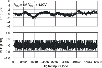 Figure 2. Linearity Error and Differential Linearity Error vs Digital Input Code (–40°C)
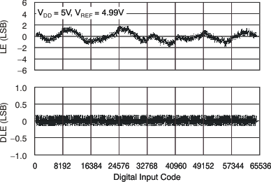 Figure 4. Linearity Error and Differential Linearity Error vs Digital Input Code (125°C)
 Figure 6. Full-Scale Error vs Temperature
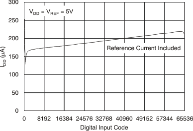 Figure 8. Supply Current vs Digital Input Code
 Figure 10. Supply Current vs Supply Voltage
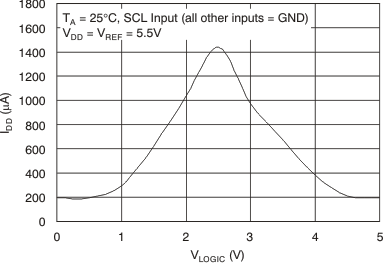 Figure 12. Supply Current vs Logic Input Voltage
 Figure 14. Full-Scale Settling Time: 5-V Falling Edge
 Figure 16. Half-Scale Settling Time: 5-V Falling Edge
 Figure 18. Glitch Impulse: 5 V, 1-LSB Step, Falling Edge
 Figure 20. Glitch Impulse: 5 V, 16-LSB Step, Falling Edge
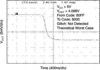 Figure 22. Glitch Impulse: 5 V, 256-LSB Step, Falling Edge
 Figure 24. Signal-to-Noise Ratio vs Output Frequency
 Figure 26. Output Noise Density
 Figure 3. Linearity Error and Differential Linearity Error vs Digital Input Code (25°C)
 Figure 5. Offset Error vs Temperature
 Figure 7. Source and Sink Current Capability
 Figure 9. Power-Supply Current vs Temperature
 Figure 11. Power-Down Current vs Supply Voltage
 Figure 13. Full-Scale Settling Time: 5-V Rising Edge
 Figure 15. Half-Scale Settling Time: 5-V Rising Edge
 Figure 17. Glitch Impulse: 5 V, 1-LSB Step, Rising Edge
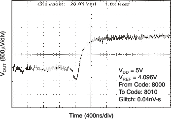 Figure 19. Glitch Impulse: 5 V, 16-LSB Step, Rising Edge
 Figure 21. Glitch Impulse: 5 V, 256-LSB Step, Rising Edge
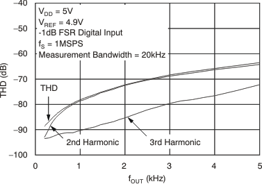 Figure 23. Total Harmonic Distortion vs Output Frequency
 Figure 25. Power Spectral Density
