SLAS464C
December 2006 – January 2018
DAC8560
PRODUCTION DATA.
1
Features
2
Applications
3
Description
Device Images
Functional Block Diagram
4
Revision History
5
Pin Configuration and Functions
Pin Functions
6
Specifications
6.1
Absolute Maximum Ratings
6.2
ESD Ratings
6.3
Recommended Operating Conditions
6.4
Thermal Information
6.5
Electrical Characteristics
6.6
Timing Requirements
6.7
Typical Characteristics: Internal Reference
6.8
Typical Characteristics: DAC at VDD = 5 V
6.9
Typical Characteristics: DAC at VDD = 3.6 V
6.10
Typical Characteristics: DAC at VDD = 2.7 V
7
Detailed Description
7.1
Overview
7.2
Functional Block Diagram
7.3
Feature Description
7.3.1
Digital-to-Analog Converter (DAC)
7.3.2
Resistor String
7.3.3
Output Amplifier
7.3.4
DAC Noise Performance
7.3.5
Internal Reference
7.3.5.1
Enable/Disable Internal Reference
7.3.5.2
Internal Reference Load
7.3.5.2.1
Supply Voltage
7.3.5.2.2
Temperature Drift
7.3.5.2.3
Noise Performance
7.3.5.2.4
Load Regulation
7.3.5.2.5
Long-Term Stability
7.3.5.2.6
Thermal Hysteresis
7.4
Device Functional Modes
7.4.1
Power-Down Modes
7.5
Programming
7.5.1
Serial Interface
7.5.2
Input Shift Register
7.5.3
SYNC Interrupt
7.5.4
Power-On Reset
7.6
Register Maps
7.6.1
Write Sequence for Disabling the DAC8560 Internal Reference
Table 1.
Write Sequence for Disabling the DAC8560 Internal Reference
7.6.2
Enabling the DAC8560 Internal Reference (Write Sequence 1 of 2)
Table 2.
Enabling the DAC8560 Internal Reference (Write Sequence 1 of 2)
7.6.3
Enabling the DAC8560 Internal Reference (Write Sequence 2 of 2)
Table 3.
Enabling the DAC8560 Internal Reference (Write Sequence 2 of 2)
7.6.4
DAC8560 Data Input Register Format
Table 4.
DAC8560 Data Input Register Format
8
Application and Implementation
8.1
Application Information
8.2
Typical Applications
8.2.1
Design Requirements
8.2.2
Detailed Design Procedure or Bipolar Operation > ±VREF
8.2.2.1
Bipolar Operation Greater Than ±VREF
8.2.2.1.1
Passive Component Selection
8.2.2.1.2
Amplifier Selection
8.2.2.2
Microprocessor Interfacing
8.2.2.2.1
DAC8560 to 8051 Interface
8.2.2.2.2
DAC8560 to Microwire Interface
8.2.2.2.3
DAC8560 to 68HC11 Interface
8.2.3
Application Curves
9
Power Supply Recommendations
10
Layout
10.1
Layout Guidelines
10.2
Layout Example
11
Device and Documentation Support
11.1
Documentation Support
11.1.1
Related Documentation
11.2
Receiving Notification of Documentation Updates
11.3
Community Resource
11.4
Trademarks
11.5
Electrostatic Discharge Caution
11.6
Glossary
12
Mechanical, Packaging, and Orderable Information
Package Options
Mechanical Data (Package|Pins)
DGK|8
MPDS028E
Thermal pad, mechanical data (Package|Pins)
Orderable Information
slas464c_oa
slas464c_pm
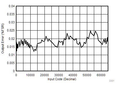
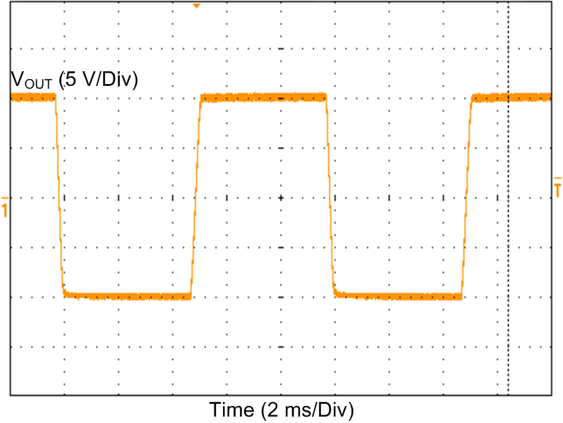
8.2.3
Application Curves
Figure 76.
Output Voltage Error vs Input Code
Figure 77.
Full-Scale Step Response