SLAS464C December   2006  – January 2018 DAC8560

PRODUCTION DATA.  

  1. Features
  2. Applications
  3. Description
    1.     Device Images
      1.      Functional Block Diagram
  4. Revision History
  5. Pin Configuration and Functions
    1.     Pin Functions
  6. Specifications
    1. 6.1  Absolute Maximum Ratings
    2. 6.2  ESD Ratings
    3. 6.3  Recommended Operating Conditions
    4. 6.4  Thermal Information
    5. 6.5  Electrical Characteristics
    6. 6.6  Timing Requirements
    7. 6.7  Typical Characteristics: Internal Reference
    8. 6.8  Typical Characteristics: DAC at VDD = 5 V
    9. 6.9  Typical Characteristics: DAC at VDD = 3.6 V
    10. 6.10 Typical Characteristics: DAC at VDD = 2.7 V
  7. Detailed Description
    1. 7.1 Overview
    2. 7.2 Functional Block Diagram
    3. 7.3 Feature Description
      1. 7.3.1 Digital-to-Analog Converter (DAC)
      2. 7.3.2 Resistor String
      3. 7.3.3 Output Amplifier
      4. 7.3.4 DAC Noise Performance
      5. 7.3.5 Internal Reference
        1. 7.3.5.1 Enable/Disable Internal Reference
        2. 7.3.5.2 Internal Reference Load
          1. 7.3.5.2.1 Supply Voltage
          2. 7.3.5.2.2 Temperature Drift
          3. 7.3.5.2.3 Noise Performance
          4. 7.3.5.2.4 Load Regulation
          5. 7.3.5.2.5 Long-Term Stability
          6. 7.3.5.2.6 Thermal Hysteresis
    4. 7.4 Device Functional Modes
      1. 7.4.1 Power-Down Modes
    5. 7.5 Programming
      1. 7.5.1 Serial Interface
      2. 7.5.2 Input Shift Register
      3. 7.5.3 SYNC Interrupt
      4. 7.5.4 Power-On Reset
    6. 7.6 Register Maps
      1. 7.6.1 Write Sequence for Disabling the DAC8560 Internal Reference
        1. Table 1. Write Sequence for Disabling the DAC8560 Internal Reference
      2. 7.6.2 Enabling the DAC8560 Internal Reference (Write Sequence 1 of 2)
        1. Table 2. Enabling the DAC8560 Internal Reference (Write Sequence 1 of 2)
      3. 7.6.3 Enabling the DAC8560 Internal Reference (Write Sequence 2 of 2)
        1. Table 3. Enabling the DAC8560 Internal Reference (Write Sequence 2 of 2)
      4. 7.6.4 DAC8560 Data Input Register Format
        1. Table 4. DAC8560 Data Input Register Format
  8. Application and Implementation
    1. 8.1 Application Information
    2. 8.2 Typical Applications
      1. 8.2.1 Design Requirements
      2. 8.2.2 Detailed Design Procedure or Bipolar Operation > ±VREF
        1. 8.2.2.1 Bipolar Operation Greater Than ±VREF
          1. 8.2.2.1.1 Passive Component Selection
          2. 8.2.2.1.2 Amplifier Selection
        2. 8.2.2.2 Microprocessor Interfacing
          1. 8.2.2.2.1 DAC8560 to 8051 Interface
          2. 8.2.2.2.2 DAC8560 to Microwire Interface
          3. 8.2.2.2.3 DAC8560 to 68HC11 Interface
      3. 8.2.3 Application Curves
  9. Power Supply Recommendations
  10. 10Layout
    1. 10.1 Layout Guidelines
    2. 10.2 Layout Example
  11. 11Device and Documentation Support
    1. 11.1 Documentation Support
      1. 11.1.1 Related Documentation
    2. 11.2 Receiving Notification of Documentation Updates
    3. 11.3 Community Resource
    4. 11.4 Trademarks
    5. 11.5 Electrostatic Discharge Caution
    6. 11.6 Glossary
  12. 12Mechanical, Packaging, and Orderable Information

Package Options

Mechanical Data (Package|Pins)
Thermal pad, mechanical data (Package|Pins)
Orderable Information

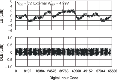
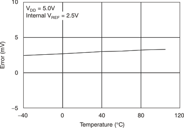
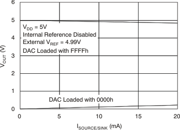
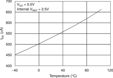
Typical Characteristics: DAC at VDD = 5 V

At TA = 25°C, external reference used, and DAC output not loaded, unless otherwise noted.
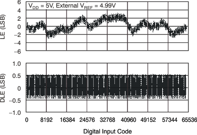
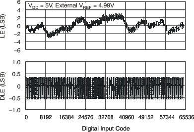
DAC8560 tc_le_40c_5v_las464.gif
–40°C
Figure 14. Linearity Error and Differential Linearity Error vs Digital Input Code
DAC8560 tc_le_105c_5v_las464.gif
105°C
Figure 16. Linearity Error and Differential Linearity Error vs Digital Input Code
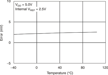
DAC8560 tc_fse-tmp_5v_las464.gif
Figure 18. Full-Scale Error vs Temperature
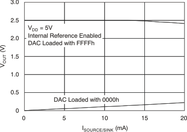
DAC8560 tc_source_sink_5v_dis_las464.gif
Figure 20. Source and Sink Current Capability
DAC8560 tc_idd-tmp_5v_las464.gif
Figure 22. Power-Supply Current vs Temperature
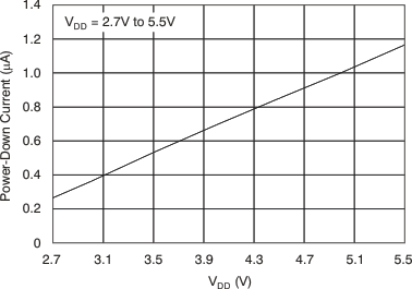
DAC8560 tc_pd_vdd_5v_las464.gif
Figure 24. Power-Down Current vs Power-Supply Voltage
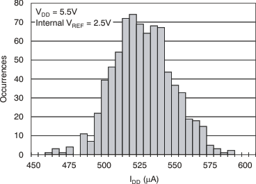
DAC8560 tc_histo_5v_las464.gif
Figure 26. Power-Supply Current Histogram
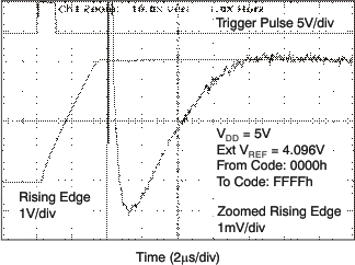
DAC8560 tc_fs_5v_ris_las464.gif
5-V Rising Edge
Figure 28. Full-Scale Settling Time
DAC8560 tc_hs_5v_ris_las464.gif
5-V Rising Edge
Figure 30. Half-Scale Settling Time
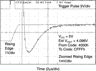
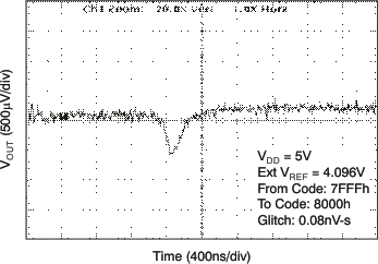
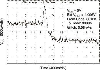
DAC8560 tc_gl_5v1_ris_las464.gif
Rising Edge 5 V 1-LSB Step
Figure 32. Glitch Energy
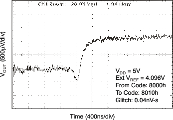
DAC8560 tc_gl_5v16_ris_las464.gif
Rising Edge 5 V 16-LSB Step
Figure 34. Glitch Energy
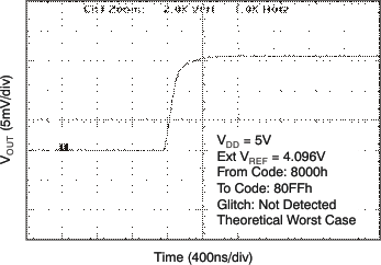
DAC8560 tc_gl_5v256_ris_las464.gif
Rising Edge 5 V 2566-LSB Step
Figure 36. Glitch Energy
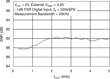
DAC8560 tc_snr-fout_5v_las464.gif
Figure 38. Signal-to-Noise Ratio vs Output Frequency
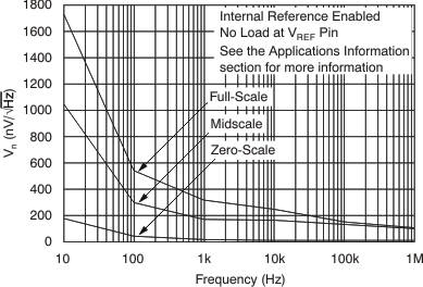
DAC8560 tc_noise-freq_no_las464.gif
Explained in more detail in Application and Implementation.
Figure 40. DAC Output Noise Density vs Frequency
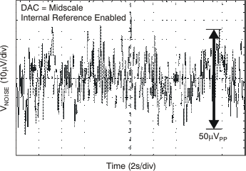
DAC8560 tc_ref_noise_las464.gif
0.1 Hz to 10 Hz
Figure 42. DAC Output Noise
DAC8560 tc_le_25c_5v_las464.gif
25°C
Figure 15. Linearity Error and Differential Linearity Error vs Digital Input Code
DAC8560 tc_zse-tmp_5v_las464.gif
Figure 17. Zero-Scale Error vs Temperature
DAC8560 tc_source_sink_5v_en_las464.gif
Figure 19. Source and Sink Current Capability
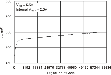
DAC8560 tc_idd-code_5v_las464.gif
Figure 21. Power-Supply Current vs Digital Input Code
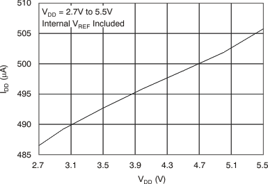
DAC8560 tc_idd_vdd_5v_las464.gif
Figure 23. Power-Supply Current vs Power-Supply Voltage
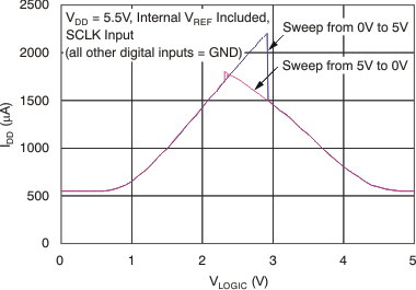
DAC8560 tc_idd-logic_5v_las464.gif
Figure 25. Power-Supply Current vs Logic Input Voltage
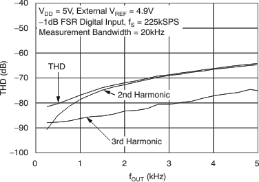
DAC8560 tc_thd-fout_5v_las464.gif
Figure 27. Total Harmonic Distortion vs Output Frequency
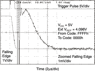
DAC8560 tc_fs_5v_fal_las464.gif
5-V Falling Edge
Figure 29. Full-Scale Settling Time
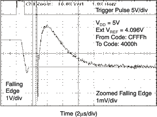
DAC8560 tc_hs_5v_fal_las464.gif
5-V Falling Edge
Figure 31. Half-Scale Settling Time
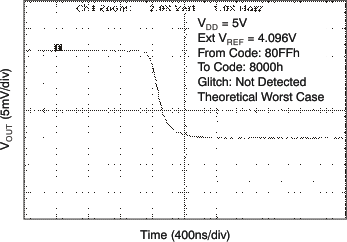
DAC8560 tc_gl_5v1_fal_las464.gif
Falling Edge 5 V 1-LSB Step
Figure 33. Glitch Energy
DAC8560 tc_gl_5v16_fal_las464.gif
Falling Edge 5 V 16-LSB Step
Figure 35. Glitch Energy
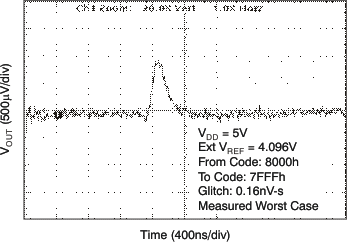
DAC8560 tc_gl_5v256_fal_las464.gif
Falling Edge 5 V 256-LSB Step
Figure 37. Glitch Energy
DAC8560 tc_pwr_den_5v_las464.gif
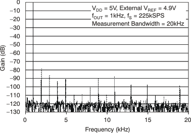
Figure 39. Power Spectral Density
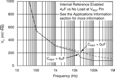
DAC8560 tc_noise-freq_4uf_las464.gif
Explained in more detail in the Application and Implementation
Figure 41. DAC Output Noise Density vs Frequency