SLAS950A May 2013 – June 2015 DAC7562-Q1 , DAC7563-Q1 , DAC8162-Q1 , DAC8163-Q1 , DAC8562-Q1 , DAC8563-Q1
PRODUCTION DATA.
- 1 Features
- 2 Applications
- 3 Description
- 4 Revision History
- 5 Device Comparison Table
- 6 Pin Configuration and Functions
- 7 Specifications
- 8 Detailed Description
- 9 Application and Implementation
- 10Power Supply Recommendations
- 11Layout
- 12Device and Documentation Support
- 13Mechanical, Packaging, and Orderable Information
Package Options
Mechanical Data (Package|Pins)
- DGS|10
Thermal pad, mechanical data (Package|Pins)
Orderable Information
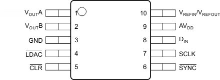
6 Pin Configuration and Functions
DGS Package
10-Pin VSSOP
Top View

Pin Functions
| PIN | DESCRIPTION | |
|---|---|---|
| NAME | NO. | |
| AVDD | 9 | Power-supply input, 2.7 V to 5.5 V |
| CLR | 5 | Asynchronous clear input. The CLR input is falling-edge sensitive. When CLR is activated, zero scale (DACxx62-Q1) or mid-scale (DACxx63-Q1) is loaded to all input and DAC registers. This sets the DAC output voltages accordingly. The part exits clear code mode on the 24th falling edge of the next write to the part. If CLR is activated during a write sequence, the write is aborted. |
| DIN | 8 | Serial data input. Data are clocked into the 24-bit input shift register on each falling edge of the serial clock input. Schmitt-trigger logic input |
| GND | 3 | Ground reference point for all circuitry on the device |
| LDAC | 4 | In synchronous mode, data are updated with the falling edge of the 24th SCLK cycle, which follows a falling edge of SYNC. For such synchronous updates, the LDAC pin is not required, and it must be connected to GND permanently or asserted and held low before sending commands to the device. In asynchronous mode, the LDAC pin is used as a negative edge-triggered timing signal for simultaneous DAC updates. Multiple single-channel commands can be written in order to set different channel buffers to desired values and then make a falling edge on LDAC pin to simultaneously update the DAC output registers. |
| SCLK | 7 | Serial clock input. Data can be transferred at rates up to 50 MHz. Schmitt-trigger logic input |
| SYNC | 6 | Level-triggered control input (active-low). This input is the frame synchronization signal for the input data. When SYNC goes low, it enables the input shift register, and data are sampled on subsequent falling clock edges. The DAC output updates following the 24th clock falling edge. If SYNC is taken high before the 23rd clock edge, the rising edge of SYNC acts as an interrupt, and the write sequence is ignored by the DAC756x-Q1, DAC816x-Q1, DAC856x-Q1. Schmitt-trigger logic input |
| VOUTA | 1 | Analog output voltage from DAC-A |
| VOUTB | 2 | Analog output voltage from DAC-B |
| VREFIN/VREFOUT | 10 | Bidirectional voltage reference pin. If internal reference is used, 2.5-V output. |