SLAS719E August   2010  – June 2015 DAC7562 , DAC7563 , DAC8162 , DAC8163 , DAC8562 , DAC8563

PRODUCTION DATA.  

  1. Features
  2. Applications
  3. Description
  4. Revision History
  5. Device Comparison Table
  6. Pin Configuration and Functions
  7. Specifications
    1. 7.1 Absolute Maximum Ratings
    2. 7.2 ESD Ratings
    3. 7.3 Recommended Operating Conditions
    4. 7.4 Thermal Information
    5. 7.5 Electrical Characteristics
    6. 7.6 Timing Requirements
    7. 7.7 Typical Characteristics
      1. 7.7.1 Typical Characteristics: Internal Reference
      2. 7.7.2 Typical Characteristics: DAC at AVDD = 5.5 V
      3. 7.7.3 Typical Characteristics: DAC at AVDD = 3.6 V
      4. 7.7.4 Typical Characteristics: DAC at AVDD = 2.7 V
  8. Detailed Description
    1. 8.1 Overview
    2. 8.2 Functional Block Diagram
    3. 8.3 Feature Description
      1. 8.3.1 Digital-to-Analog Converter (DAC)
        1. 8.3.1.1 Resistor String
        2. 8.3.1.2 Output Amplifier
      2. 8.3.2 Internal Reference
      3. 8.3.3 Power-On Reset
        1. 8.3.3.1 Power-On Reset to Zero-Scale
        2. 8.3.3.2 Power-On Reset to Mid-Scale
        3. 8.3.3.3 Power-On Reset (POR) Levels
    4. 8.4 Device Functional Modes
      1. 8.4.1 Power-Down Modes
        1. 8.4.1.1 DAC Power-Down Commands
      2. 8.4.2 Gain Function
      3. 8.4.3 Software Reset Function
      4. 8.4.4 Internal Reference Enable Register
        1. 8.4.4.1 Enabling Internal Reference
        2. 8.4.4.2 Disabling Internal Reference
      5. 8.4.5 CLR Functionality
      6. 8.4.6 LDAC Functionality
    5. 8.5 Programming
      1. 8.5.1 SYNC Interrupt
      2. 8.5.2 DAC Register Configuration
  9. Application and Implementation
    1. 9.1 Application Information
      1. 9.1.1 DAC Internal Reference
        1. 9.1.1.1 Supply Voltage
        2. 9.1.1.2 Temperature Drift
        3. 9.1.1.3 Noise Performance
        4. 9.1.1.4 Load Regulation
          1. 9.1.1.4.1 Long-Term Stability
        5. 9.1.1.5 Thermal Hysteresis
      2. 9.1.2 DAC Noise Performance
    2. 9.2 Typical Applications
      1. 9.2.1 Combined Voltage and Current Analog Output Module Using the XTR300
        1. 9.2.1.1 Design Requirements
        2. 9.2.1.2 Detailed Design Procedure
        3. 9.2.1.3 Application Curves
      2. 9.2.2 Up to ±15-V Bipolar Output Using the DAC8562
    3. 9.3 System Examples
      1. 9.3.1 MSP430 Microprocessor Interfacing
      2. 9.3.2 TMS320 McBSP Microprocessor Interfacing
      3. 9.3.3 OMAP-L1x Processor Interfacing
  10. 10Power Supply Recommendations
  11. 11Layout
    1. 11.1 Layout Guidelines
    2. 11.2 Layout Example
  12. 12Device and Documentation Support
    1. 12.1 Related Links
    2. 12.2 Community Resources
    3. 12.3 Trademarks
    4. 12.4 Electrostatic Discharge Caution
    5. 12.5 Glossary
  13. 13Mechanical, Packaging, and Orderable Information

Package Options

Mechanical Data (Package|Pins)
Thermal pad, mechanical data (Package|Pins)
Orderable Information

7 Specifications

7.1 Absolute Maximum Ratings(1)

Over operating ambient temperature range (unless otherwise noted).
MIN MAX UNIT
AVDD to GND –0.3 6 V
CLR, DIN, LDAC, SCLK and SYNC input voltage to GND –0.3 AVDD + 0.3 V
VOUT[A, B] to GND –0.3 AVDD + 0.3 V
VREFIN/VREFOUT to GND –0.3 AVDD + 0.3 V
Operating temperature range –40 125 °C
Junction temperature, TJ 150 °C
Storage temperature, Tstg –65 150 °C
(1) Stresses beyond those listed under Absolute Maximum Ratings may cause permanent damage to the device. These are stress ratings only, and do not imply functional operation of the device at these or any other conditions beyond those indicated under Recommended Operating Conditions. Exposure to absolute-maximum-rated conditions for extended periods may affect device reliability.

7.2 ESD Ratings

VALUE UNIT
V(ESD) Electrostatic discharge Human-body model (HBM), per ANSI/ESDA/JEDEC JS-001(1) ±1000 V
Charged-device model (CDM), per JEDEC specification JESD22-C101(2) ±500
(1) JEDEC document JEP155 states that 500-V HBM allows safe manufacturing with a standard ESD control process.
(2) JEDEC document JEP157 states that 250-V CDM allows safe manufacturing with a standard ESD control process.

7.3 Recommended Operating Conditions

over operating ambient temperature range (unless otherwise noted)
MIN NOM MAX UNIT
POWER SUPPLY
Supply voltage AVDD to GND 2.7 5.5 V
DIGITAL INPUTS
Digital input voltage CLR, DIN, LDAC, SCLK and SYNC 0 AVDD V
REFERENCE INPUT
VREFIN Reference input voltage 0 AVDD V
TEMPERATURE RANGE
TA Operating ambient temperature –40 125 °C

7.4 Thermal Information

THERMAL METRIC DAC756x, DAC816x, DAC856x UNIT
DSC (WSON) DGS (VSSOP)
10 PINS 10 PINS
RθJA Junction-to-ambient thermal resistance 62.8 173.8 °C/W
RθJC(top) Junction-to-case (top) thermal resistance 44.3 48.5 °C/W
RθJB Junction-to-board thermal resistance 26.5 79.9 °C/W
ψJT Junction-to-top characterization parameter 0.4 1.7 °C/W
ψJB Junction-to-board characterization parameter 25.5 68.4 °C/W
RθJC(bot) Junction-to-case (bottom) thermal resistance 46.2 N/A °C/W

7.5 Electrical Characteristics

At AVDD = 2.7 V to 5.5 V and TA = –40°C to 125°C (unless otherwise noted).
PARAMETER TEST CONDITIONS MIN TYP MAX UNIT
STATIC PERFORMANCE(1)
DAC856x Resolution 16 Bits
Relative accuracy Using line passing through codes 512 and 65,024 ±4 ±12 LSB
Differential nonlinearity 16-bit monotonic ±0.2 ±1 LSB
DAC816x Resolution 14 Bits
Relative accuracy Using line passing through codes 128 and 16,256 ±1 ±3 LSB
Differential nonlinearity 14-bit monotonic ±0.1 ±0.5 LSB
DAC756x Resolution 12 Bits
Relative accuracy Using line passing through codes 32 and 4,064 ±0.3 ±0.75 LSB
Differential nonlinearity 12-bit monotonic ±0.05 ±0.25 LSB
Offset error Extrapolated from two-point line(1), unloaded ±1 ±4 mV
Offset error drift ±2 µV/°C
Full-scale error DAC register loaded with all 1s ±0.03 ±0.2 % FSR
Zero-code error DAC register loaded with all 0s 1 4 mV
Zero-code error drift ±2 µV/°C
Gain error Extrapolated from two-point line(1), unloaded ±0.01 ±0.15 % FSR
Gain temperature coefficient ±1 ppm FSR/°C
OUTPUT CHARACTERISTICS(2)
Output voltage range 0 AVDD V
Output voltage settling time(3) DACs unloaded 7 µs
RL = 1 MΩ 10
Slew rate Measured between 20%–80% of a full-scale transition 0.75 V/µs
Capacitive load stability RL = ∞ 1 nF
RL = 2 kΩ 3
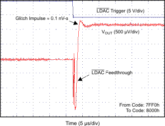
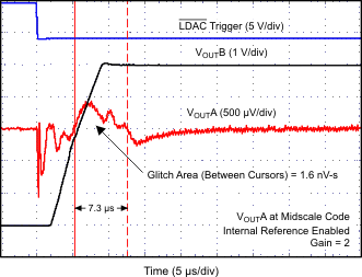
Code-change glitch impulse 1-LSB change around major carry 0.1 nV-s
Digital feedthrough SCLK toggling, SYNC high 0.1 nV-s
Power-on glitch impulse RL = 2 kΩ, CL = 470 pF, AVDD = 5.5 V 40 mV
Channel-to-channel dc crosstalk Full-scale swing on adjacent channel,
External reference
5 µV
Full-scale swing on adjacent channel,
Internal reference
15
DC output impedance At mid-scale input 5 Ω
Short-circuit current DAC outputs at full-scale, DAC outputs shorted to GND 40 mA
Power-up time, including settling time Coming out of power-down mode 50 µs
AC PERFORMANCE(2)
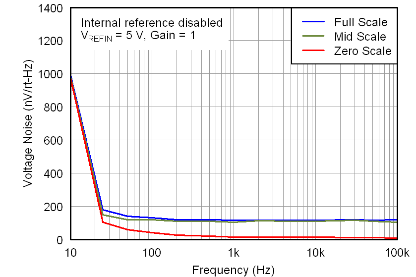
DAC output noise density TA = 25°C, at mid-scale input, fOUT = 1 kHz 90 nV/√Hz
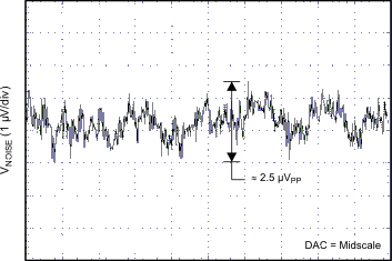
DAC output noise TA = 25°C, at mid-scale input, 0.1 Hz to 10 Hz 2.6 µVPP
LOGIC INPUTS(2)
Input-pin leakage current –1 ±0.1 1 µA
Logic input LOW voltage VIL 0 0.8 V
Logic input HIGH voltage VIH 0.7 × AVDD AVDD V
Pin capacitance 3 pF
REFERENCE
External reference current External VREF = 2.5 V (when internal reference is disabled), all channels active using gain = 1 15 µA
Reference input impedance Internal reference disabled, gain = 1 170
Internal reference disabled, gain = 2 85
REFERENCE OUTPUT
Output voltage TA = 25°C 2.495 2.5 2.505 V
Initial accuracy TA = 25°C –5 ±0.1 5 mV
Output-voltage temperature drift 4 10 ppm/°C
Output-voltage noise f = 0.1 Hz to 10 Hz 12 µVPP
Output-voltage noise density (high-frequency noise) TA = 25°C, f = 1 kHz, CL = 0 µF 250 nV/√Hz
TA = 25°C, f = 1 MHz, CL = 0 µF 30
TA = 25°C, f = 1 MHz, CL = 4.7 µF 10
Load regulation, sourcing(4) TA = 25°C 20 µV/mA
Load regulation, sinking(4) TA = 25°C 185 µV/mA
Output-current load capability(2) ±20 mA
Line regulation TA = 25°C 50 µV/V
Long-term stability or drift (aging)(4) TA = 25°C, time = 0 to 1900 hours 100 ppm
Thermal hysteresis(4) First cycle 200 ppm
Additional cycles 50
POWER REQUIREMENTS(5)
Power supply current (IDD) AVDD = 3.6 V to 5.5 V, normal mode, internal reference off 0.25 0.5 mA
AVDD = 3.6 V to 5.5 V, normal mode, internal reference on 0.9 1.6
AVDD = 3.6 V to 5.5 V, power-down modes(6) 0.55 2 µA
AVDD = 3.6 V to 5.5 V, power-down modes 0.55 4
AVDD = 2.7 V to 3.6 V, normal mode, internal reference off 0.2 0.4 mA
AVDD = 2.7 V to 3.6 V, normal mode, internal reference on 0.73 1.4
AVDD = 2.7 V to 3.6 V, power-down modes(6) 0.35 2 µA
AVDD = 2.7 V to 3.6 V, power-down modes 0.35 3
Power dissipation AVDD = 3.6 V to 5.5 V, normal mode, internal reference off 0.9 2.75 mW
AVDD = 3.6 V to 5.5 V, normal mode, internal reference on 3.2 8.8
AVDD = 3.6 V to 5.5 V, power-down modes(6) 2 11 µW
AVDD = 3.6 V to 5.5 V, power-down modes 2 22
AVDD = 2.7 V to 3.6 V, normal mode, internal reference off 0.54 1.44 mW
AVDD = 2.7 V to 3.6 V, normal mode, internal reference on 1.97 5
AVDD = 2.7 V to 3.6 V, power-down modes(6) 0.95 7.2 µW
AVDD = 2.7 V to 3.6 V, power-down modes 0.95 10.8
(1) 16-bit: codes 512 and 65,024; 14-bit: codes 128 and 16,256; 12-bit: codes 32 and 4,064
(2) Specification based on design or characterization. Not production tested
(3) Transition time between 1 / 4 scale and 3 / 4 scale, including settling to within ±0.024% FSR
(4) See the Application Information section of this data sheet.
(5) Input code = mid-scale, no load, VINH = AVDD, and VINL = GND
(6) TA = –40°C to 105°C

7.6 Timing Requirements(1)(2)

At AVDD = 2.7 V to 5.5 V and over –40°C to 125°C (unless otherwise noted).
DAC756x, DAC816x, DAC856x UNIT
MIN TYP MAX
f(SCLK) Serial clock frequency 50 MHz
t(1) SCLK falling edge to SYNC falling edge (for successful write operation) 10 ns
t(2) SCLK cycle time 20 ns
t(3) SYNC rising edge to 23rd SCLK falling edge (for successful SYNC interrupt) 13 ns
t(4) Minimum SYNC HIGH time 80 ns
t(5) SYNC to SCLK falling edge setup time 13 ns
t(6) SCLK LOW time 8 ns
t(7) SCLK HIGH time 8 ns
t(8) SCLK falling edge to SYNC rising edge 10 ns
t(9) Data setup time 6 ns
t(10) Data hold time 5 ns
t(11) SCLK falling edge to LDAC falling edge for asynchronous LDAC update mode 5 ns
t(12) LDAC pulse duration, LOW time 10 ns
t(13) CLR pulse duration, LOW time 80 ns
t(14) CLR falling edge to start of VOUT transition 100 ns
(1) All input signals are specified with tr = tf = 3 ns (10% to 90% of AVDD) and timed from a voltage level of (VIL + VIH) / 2.
(2) See the Serial Write Operation timing diagram (Figure 1).
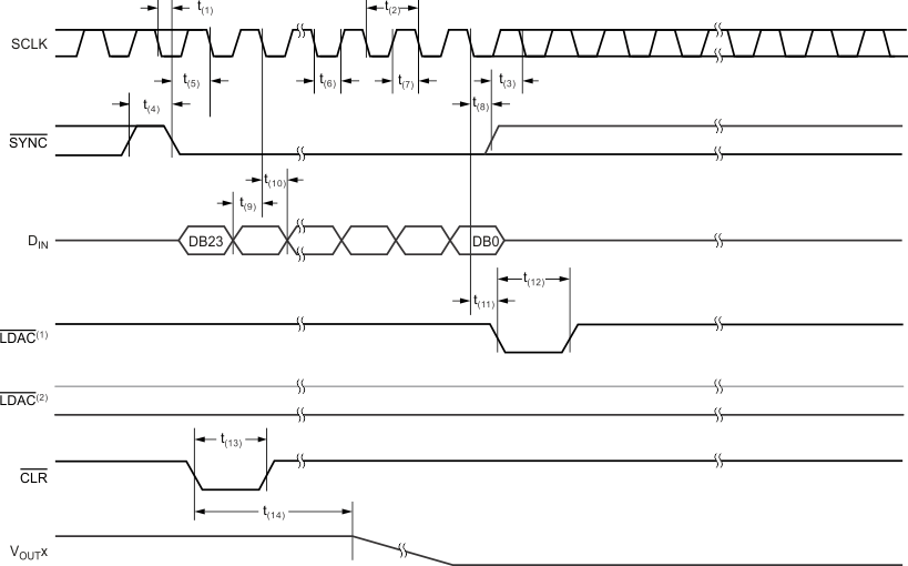
DAC7562 DAC7563 DAC8162 DAC8163 DAC8562 DAC8563 tim_ser_write_op_LAS719.gif
1. Asynchronous LDAC update mode. For more information, see the LDAC Functionality section.
2. Synchronous LDAC update mode; LDAC remains low. For more information, see the LDAC Functionality section.
Figure 1. Serial Write Operation

7.7 Typical Characteristics

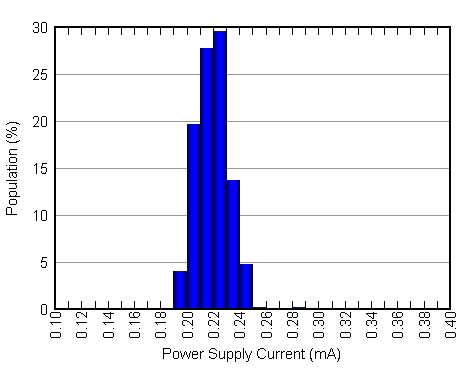
Table 1. Typical Characteristics: Internal Reference Performance

MEASUREMENT POWER-SUPPLY VOLTAGE FIGURE NUMBER
Internal Reference Voltage vs Temperature 5.5 V Figure 2
Internal Reference Voltage Temperature Drift Histogram Figure 3
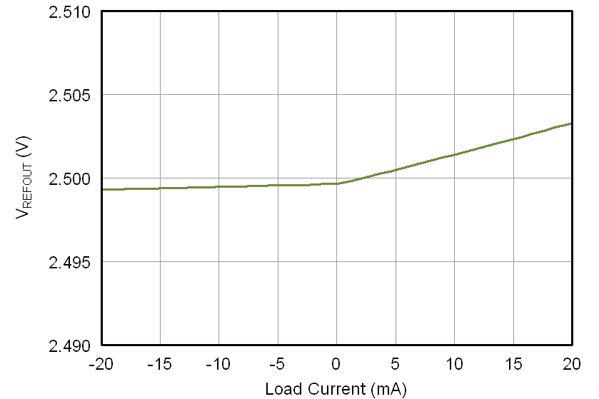
Internal Reference Voltage vs Load Current Figure 4
Internal Reference Voltage vs Time Figure 5
Internal Reference Noise Density vs Frequency Figure 6
Internal Reference Voltage vs Supply Voltage 2.7 V–5.5 V Figure 7

Table 2. Typical Characteristics: DAC Static Performance

MEASUREMENT POWER-SUPPLY VOLTAGE FIGURE NUMBER
FULL-SCALE, GAIN, OFFSET AND ZERO-CODE ERRORS
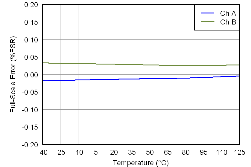
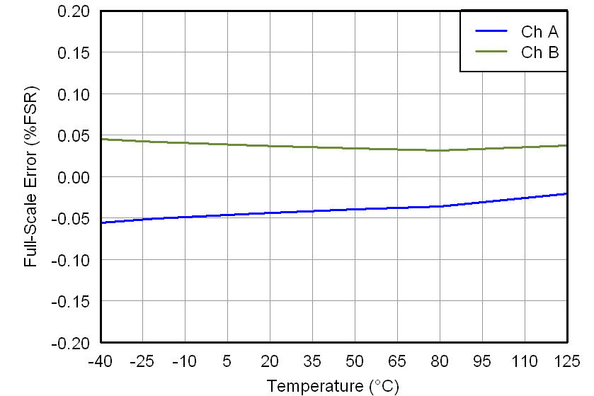
Full-Scale Error vs Temperature 5.5 V Figure 16
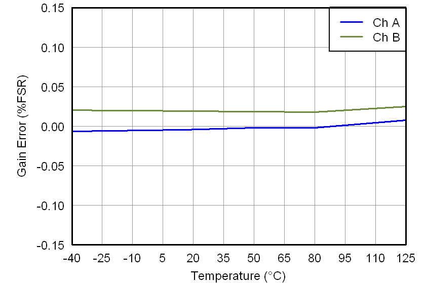
Gain Error vs Temperature Figure 17
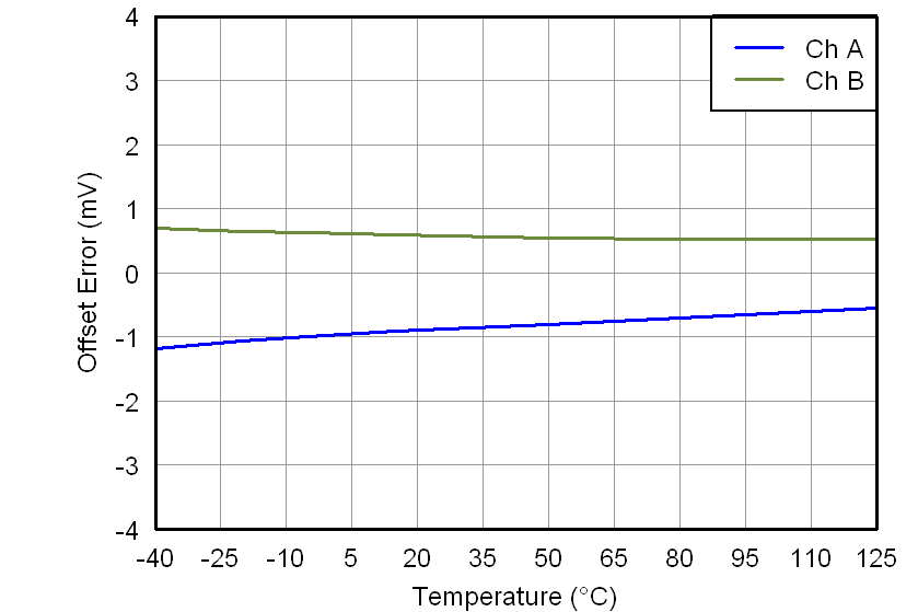
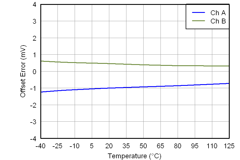
Offset Error vs Temperature Figure 18
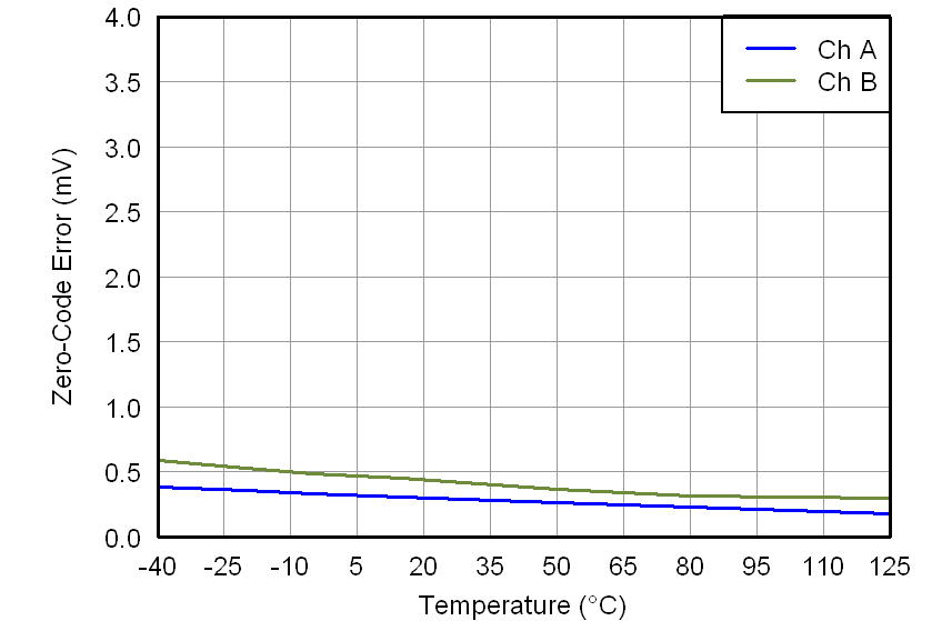
Zero-Code Error vs Temperature Figure 19
Full-Scale Error vs Temperature 2.7 V Figure 63
Gain Error vs Temperature Figure 64
Offset Error vs Temperature Figure 65
Zero-Code Error vs Temperature Figure 66
LOAD REGULATION
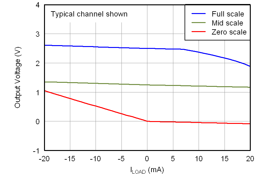
DAC Output Voltage vs Load Current 5.5 V Figure 30
2.7 V Figure 74
DIFFERENTIAL NONLINEARITY ERROR
Differential Linearity Error vs Digital Input Code T = –40°C 5.5 V Figure 9
T = 25°C Figure 11
T = 125°C Figure 13
Differential Linearity Error vs Temperature Figure 15
Differential Linearity Error vs Digital Input Code T = –40°C 2.7 V Figure 56
T = 25°C Figure 58
T = 125°C Figure 60
Differential Linearity Error vs Temperature Figure 62
INTEGRAL NONLINEARITY ERROR (RELATIVE ACCURACY)
Linearity Error vs Digital Input Code T = –40°C 5.5 V Figure 8
T = 25°C Figure 10
T = 125°C Figure 12
Linearity Error vs Temperature Figure 14
Linearity Error vs Digital Input Code T = –40°C 2.7 V Figure 55
T = 25°C Figure 57
T = 125°C Figure 59
Linearity Error vs Temperature Figure 61
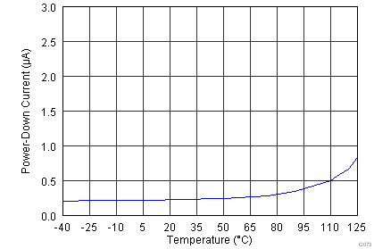
POWER-DOWN CURRENT
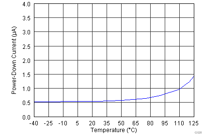
Power-Down Current vs Temperature 5.5 V Figure 28
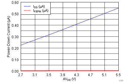
Power-Down Current vs Power-Supply Voltage 2.7 V – 5.5 V Figure 29
Power-Down Current vs Temperature 2.7 V Figure 73
POWER-SUPPLY CURRENT
Power-Supply Current vs Temperature External VREF 5.5 V Figure 20
Internal VREF Figure 21
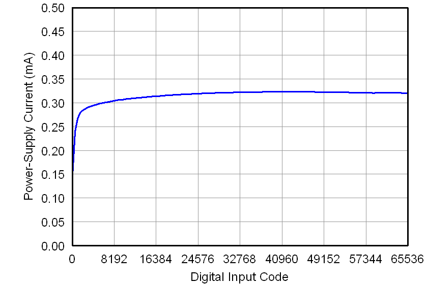
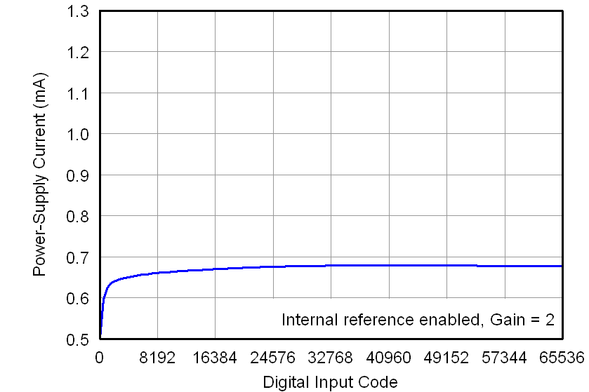
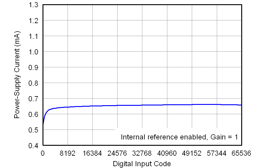
Power-Supply Current vs Digital Input Code External VREF Figure 22
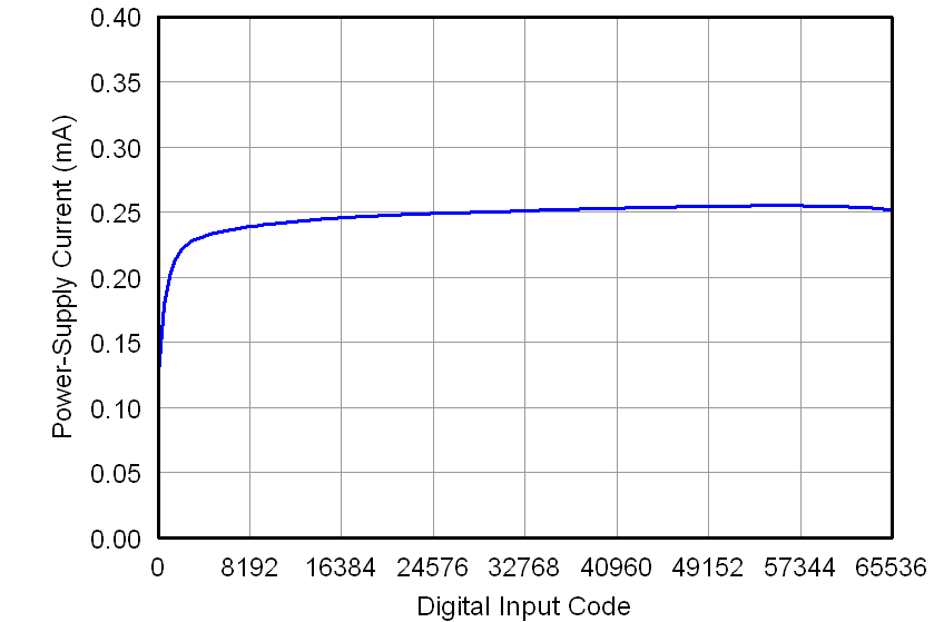
Internal VREF Figure 23
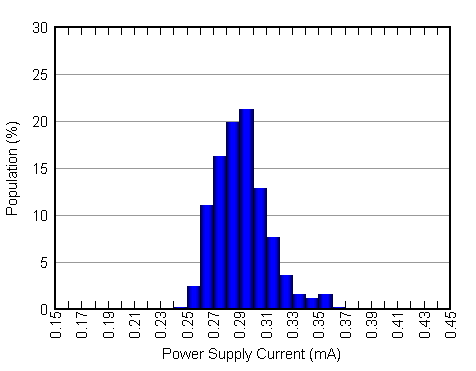
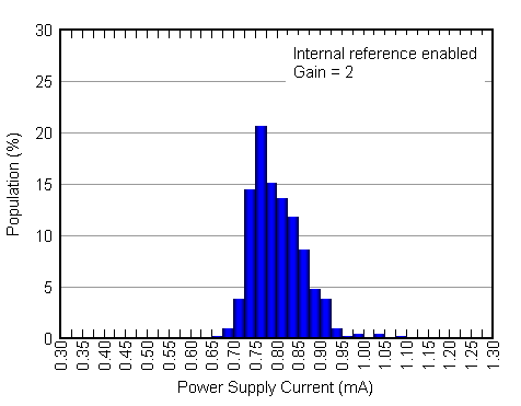
Power-Supply Current Histogram External VREF Figure 24
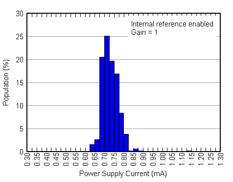
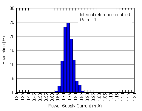
Internal VREF Figure 25
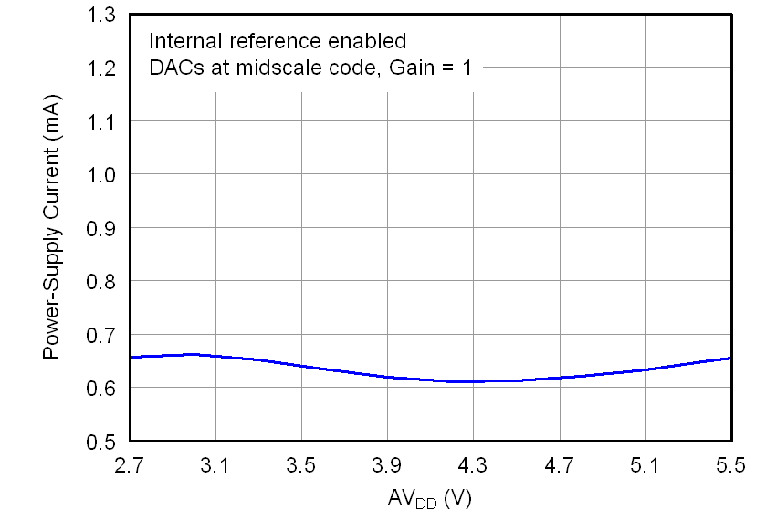
Power-Supply Current vs Power-Supply Voltage External VREF 2.7 V – 5.5 V Figure 26
Internal VREF Figure 27
Power-Supply Current vs Temperature External VREF 3.6 V Figure 49
Internal VREF Figure 50
Power-Supply Current vs Digital Input Code External VREF Figure 51
Internal VREF Figure 52
Power-Supply Current Histogram External VREF Figure 53
Internal VREF Figure 54
Power-Supply Current vs Temperature External VREF 2.7 V Figure 67
Internal VREF Figure 68
Power-Supply Current vs Digital Input Code External VREF Figure 69
Internal VREF Figure 70
Power-Supply Current Histogram External VREF Figure 71
Internal VREF Figure 72

Table 3. Typical Characteristics: DAC Dynamic Performance

MEASUREMENT POWER-SUPPLY VOLTAGE FIGURE NUMBER
CHANNEL-TO-CHANNEL CROSSTALK
Channel-to-Channel Crosstalk 5-V Rising Edge 5.5 V Figure 43
5-V Falling Edge Figure 44
CLOCK FEEDTHROUGH
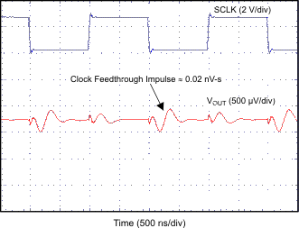
Clock Feedthrough 500 kHz, Midscale 5.5 V Figure 48
2.7 V Figure 87
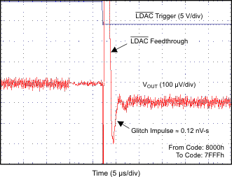
GLITCH IMPULSE
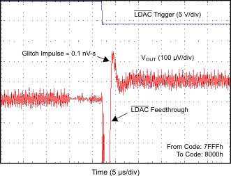
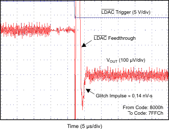
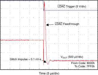
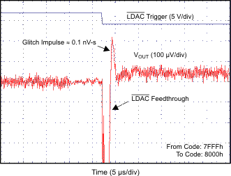
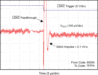
Glitch Impulse, 1-LSB Step Rising Edge, Code 7FFFh to 8000h 5.5 V Figure 37
Falling Edge, Code 8000h to 7FFFh Figure 38
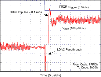
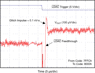
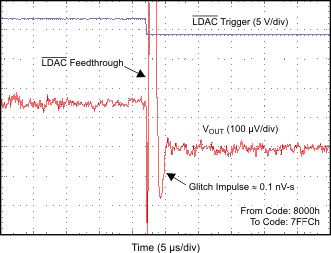
Glitch Impulse, 4-LSB Step Rising Edge, Code 7FFCh to 8000h Figure 39
Falling Edge, Code 8000h to 7FFCh Figure 40
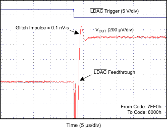
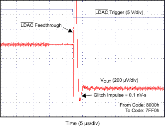
Glitch Impulse, 16-LSB Step Rising Edge, Code 7FF0h to 8000h Figure 41
Falling Edge, Code 8000h to 7FF0h Figure 42
Glitch Impulse, 1-LSB Step Rising Edge, Code 7FFFh to 8000h 2.7 V Figure 79
Falling Edge, Code 8000h to 7FFFh Figure 80
Glitch Impulse, 4-LSB Step Rising Edge, Code 7FFCh to 8000h Figure 81
Falling Edge, Code 8000h to 7FFCh Figure 82
Glitch Impulse, 16-LSB Step Rising Edge, Code 7FF0h to 8000h Figure 83
Falling Edge, Code 8000h to 7FF0h Figure 84
NOISE
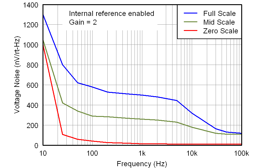
DAC Output Noise Density vs Frequency External VREF 5.5 V Figure 45
Internal VREF Figure 46
DAC Output Noise 0.1 Hz to 10 Hz External VREF Figure 47
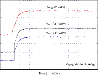
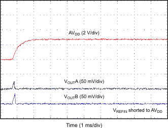
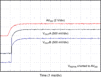
POWER-ON GLITCH
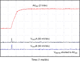
Power-On Glitch Reset to Zero Scale 5.5 V Figure 35
Reset to Midscale Figure 36
Reset to Zero Scale 2.7 V Figure 85
Reset to Midscale Figure 86
SETTLING TIME
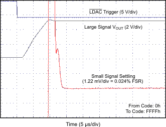
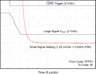
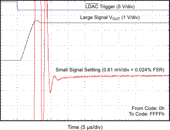
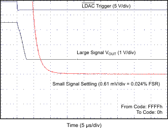
Full-Scale Settling Time Rising Edge, Code 0h to FFFFh 5.5 V Figure 31
Falling Edge, Code FFFFh to 0h Figure 32
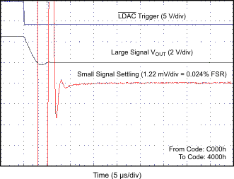
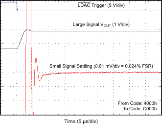
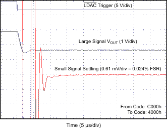
Half-Scale Settling Time Rising Edge, Code 4000h to C000h Figure 33
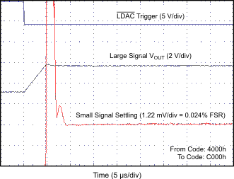
Falling Edge, Code C000h to 4000h Figure 34
Full-Scale Settling Time Rising Edge, Code 0h to FFFFh 2.7 V Figure 75
Falling Edge, Code FFFFh to 0h Figure 76
Half-Scale Settling Time Rising Edge, Code 4000h to C000h Figure 77
Falling Edge, Code C000h to 4000h Figure 78

7.7.1 Typical Characteristics: Internal Reference

At TA = 25°C, AVDD = 5.5 V, gain = 2, and VREFOUT unloaded, unless otherwise noted.
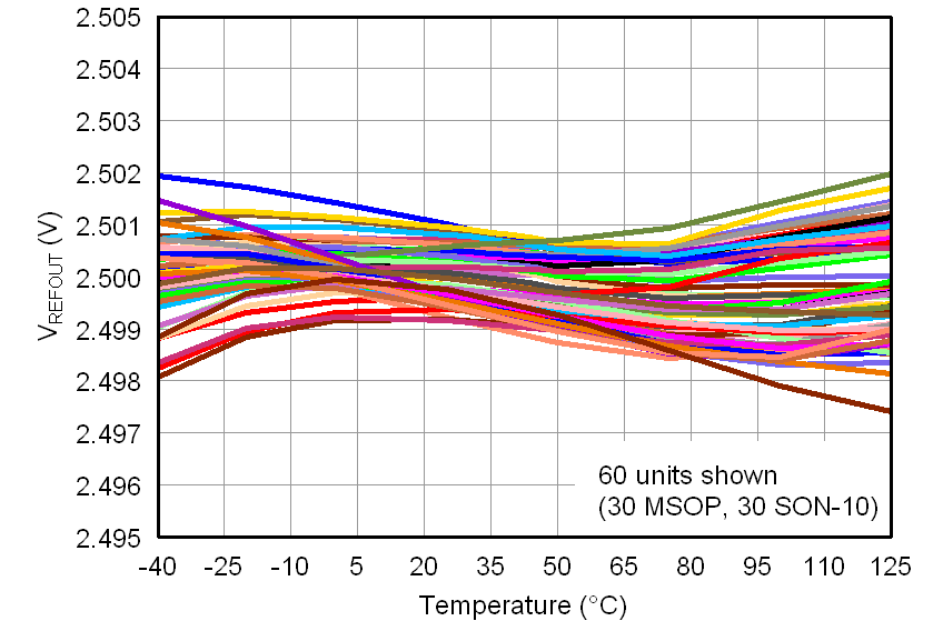
DAC7562 DAC7563 DAC8162 DAC8163 DAC8562 DAC8563 Reference_Temperature_Drift.png
Figure 2. Internal Reference Voltage vs Temperature
DAC7562 DAC7563 DAC8162 DAC8163 DAC8562 DAC8563 INTERNAL_REFERENCE_VOLTAGE_VS_LOAD_CURRENT.png
Figure 4. Internal Reference Voltage vs Load Current
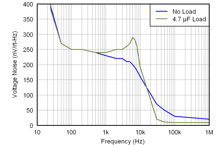
DAC7562 DAC7563 DAC8162 DAC8163 DAC8562 DAC8563 INTERNAL_REF_NOISE_DENSITY_VS_FREQUENCY.png
Figure 6. Internal Reference Noise Density vs Frequency
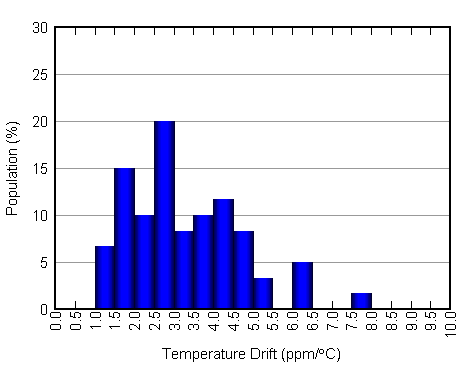
DAC7562 DAC7563 DAC8162 DAC8163 DAC8562 DAC8563 Reference_Temperature_Drift_Histogram.gif
Figure 3. Internal Reference Voltage, Temperature Drift Histogram
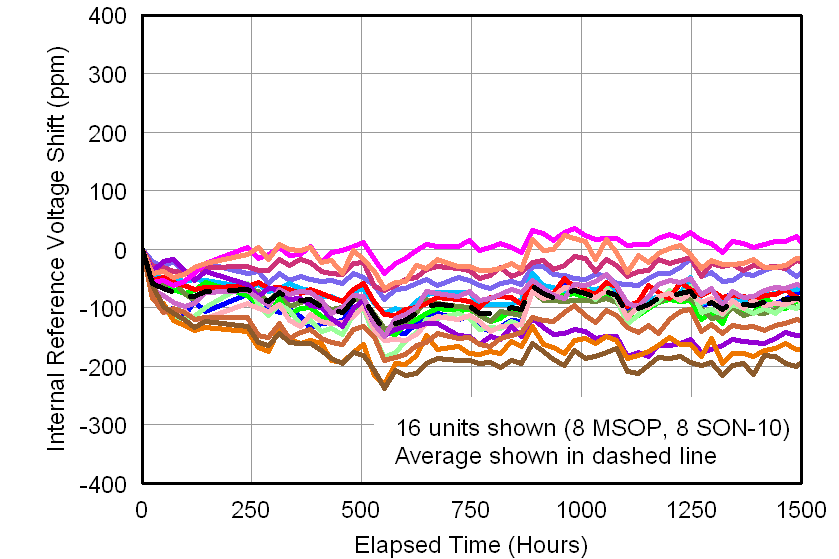
DAC7562 DAC7563 DAC8162 DAC8163 DAC8562 DAC8563 INTERNAL_REFERENCE_VOLTAGE_VS_ELAPSED_TIME.png
Figure 5. Internal Reference Voltage vs Time
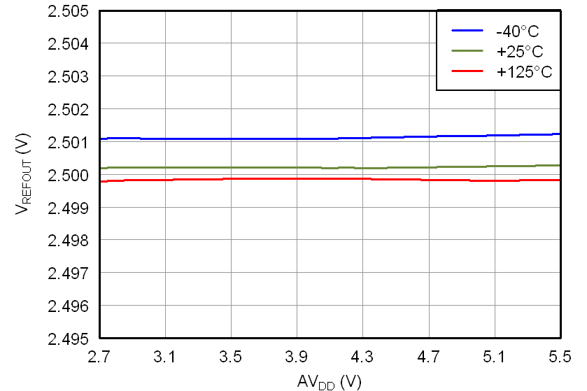
DAC7562 DAC7563 DAC8162 DAC8163 DAC8562 DAC8563 INTERNAL_REFERENCE_VOLTAGE_VS_SUPPLY_VOLTAGE.png
Figure 7. Internal Reference Voltage vs Supply Voltage

7.7.2 Typical Characteristics: DAC at AVDD = 5.5 V

At TA = 25°C, 5-V external reference used, gain = 1 and DAC output not loaded, unless otherwise noted.
DAC7562 DAC7563 DAC8162 DAC8163 DAC8562 DAC8563 5V_LINEARITY_ERRORS_VS_DIGITAL_INPUT_CODE_COLD_(INL).png
Figure 8. Linearity Error vs Digital Input Code (–40°C)
DAC7562 DAC7563 DAC8162 DAC8163 DAC8562 DAC8563 5V_LINEARITY_ERRORS_VS_DIGITAL_INPUT_CODE_ROOM_(INL).png
Figure 10. Linearity Error vs Digital Input Code (25°C)
DAC7562 DAC7563 DAC8162 DAC8163 DAC8562 DAC8563 5V_LINEARITY_ERRORS_VS_DIGITAL_INPUT_CODE_HOT_(INL).png
Figure 12. Linearity Error vs Digital Input Code (125°C)
DAC7562 DAC7563 DAC8162 DAC8163 DAC8562 DAC8563 5V_LINEARITY_ERRORS_VS_TEMPERATURE_(INL).png
Figure 14. Linearity Error vs Temperature
DAC7562 DAC7563 DAC8162 DAC8163 DAC8562 DAC8563 5V_FULL_SCALE_ERROR_VS_TEMPERATURE.png
Figure 16. Full-Scale Error vs Temperature
DAC7562 DAC7563 DAC8162 DAC8163 DAC8562 DAC8563 5V_OFFSET_ERROR_VS_TEMPERATURE.png
Figure 18. Offset Error vs Temperature
DAC7562 DAC7563 DAC8162 DAC8163 DAC8562 DAC8563 5V_POWER_SUPPLY_CURRENT_VS_TEMPERATURE_(DACs).png
Figure 20. Power-Supply Current vs Temperature
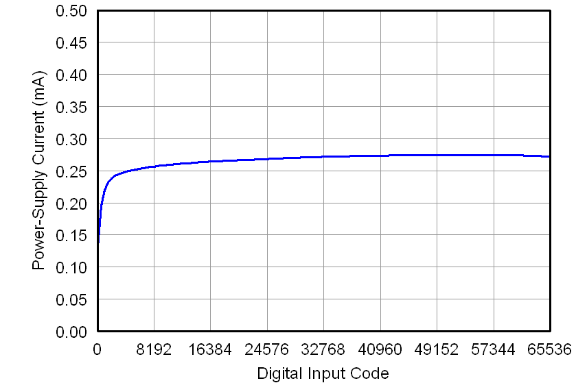
DAC7562 DAC7563 DAC8162 DAC8163 DAC8562 DAC8563 5V_IDD_VS_CODE_External_Ref.png
Figure 22. Power-Supply Current vs Digital Input Code
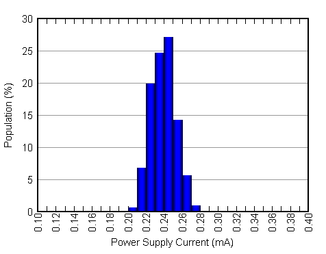
DAC7562 DAC7563 DAC8162 DAC8163 DAC8562 DAC8563 5V_IDD_EXTERNAL_REFERENCE_HISTOGRAM.gif
Figure 24. Power-Supply Current Histogram
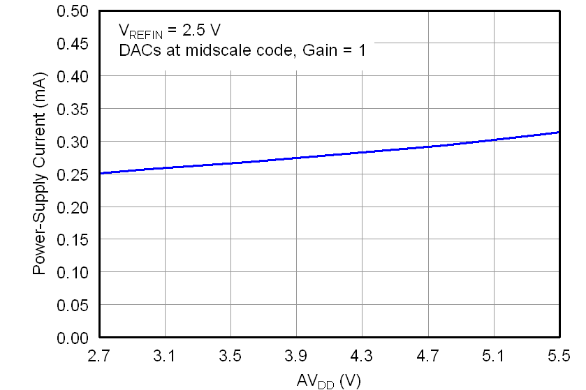
DAC7562 DAC7563 DAC8162 DAC8163 DAC8562 DAC8563 IDD_VS_VDD_External_Ref.png
Figure 26. Power-Supply Current vs Power-Supply Voltage
DAC7562 DAC7563 DAC8162 DAC8163 DAC8562 DAC8563 5V_POWER-DOWN_CURRENT_VS_TEMPERATURE_revC_si.png
Figure 28. Power-Down Current vs Temperature
DAC7562 DAC7563 DAC8162 DAC8163 DAC8562 DAC8563 5V_DAC_LOAD_CURRENT.png
Figure 30. DAC Output Voltage vs Load Current
DAC7562 DAC7563 DAC8162 DAC8163 DAC8562 DAC8563 5V_LINEARITY_ERRORS_VS_DIGITAL_INPUT_CODE_COLD_(DNL).png
Figure 9. Differential Linearity Error vs Digital Input Code (–40°C)
DAC7562 DAC7563 DAC8162 DAC8163 DAC8562 DAC8563 5V_LINEARITY_ERRORS_VS_DIGITAL_INPUT_CODE_ROOM_(DNL).png
Figure 11. Differential Linearity Error vs Digital Input Code (25°C)
DAC7562 DAC7563 DAC8162 DAC8163 DAC8562 DAC8563 5V_LINEARITY_ERRORS_VS_DIGITAL_INPUT_CODE_HOT_(DNL).png
Figure 13. Differential Linearity Error vs Digital Input Code (125°C)
DAC7562 DAC7563 DAC8162 DAC8163 DAC8562 DAC8563 5V_LINEARITY_ERRORS_VS_TEMPERATURE_(DNL).png
Figure 15. Differential Linearity Error vs Temperature
DAC7562 DAC7563 DAC8162 DAC8163 DAC8562 DAC8563 5V_GAIN_ERROR_VS_TEMPERATURE.png
Figure 17. Gain Error vs Temperature
DAC7562 DAC7563 DAC8162 DAC8163 DAC8562 DAC8563 5V_ZERO_CODE_ERROR_VS_TEMPERATURE.png
Figure 19. Zero-Code Error vs Temperature
DAC7562 DAC7563 DAC8162 DAC8163 DAC8562 DAC8563 5V_POWER_SUPPLY_CURRENT_VS_TEMPERATURE_(DACs_Reference).png
Figure 21. Power-Supply Current vs Temperature
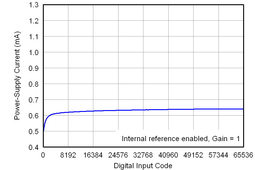
DAC7562 DAC7563 DAC8162 DAC8163 DAC8562 DAC8563 5V_IDD_VS_CODE_Internal_Ref.png
Figure 23. Power-Supply Current vs Digital Input Code
DAC7562 DAC7563 DAC8162 DAC8163 DAC8562 DAC8563 5V_IDD_INTERNAL_REFERENCE_HISTOGRAM.gif
Figure 25. Power-Supply Current Histogram
DAC7562 DAC7563 DAC8162 DAC8163 DAC8562 DAC8563 IDD_VS_VDD_Internal_Ref.png
Figure 27. Power-Supply Current vs Power-Supply Voltage
DAC7562 DAC7563 DAC8162 DAC8163 DAC8562 DAC8563 IDD_VS_VDD_POWERDOWN_revC_si.png
Figure 29. Power-Down Current vs Power-Supply Voltage
DAC7562 DAC7563 DAC8162 DAC8163 DAC8562 DAC8563 FULL-SCALE_SETTLING_TIME_5p5V_RISING_EDGE.gif
Figure 31. Full-Scale Settling Time, Rising Edge
DAC7562 DAC7563 DAC8162 DAC8163 DAC8562 DAC8563 HALF-SCALE_SETTLING_TIME_5p5V_RISING_EDGE.gif
Figure 33. Half-Scale Settling Time, Rising Edge
DAC7562 DAC7563 DAC8162 DAC8163 DAC8562 DAC8563 POWER-ON_GLITCH_RESET_TO_ZERO_SCALE_5V.gif
Figure 35. Power-On Glitch, Reset to Zero Scale
DAC7562 DAC7563 DAC8162 DAC8163 DAC8562 DAC8563 GLITCH_ENERGY_5p5V_1_LSB_RISING_EDGE.gif
Figure 37. Glitch Impulse, Rising Edge, 1-LSB Step
DAC7562 DAC7563 DAC8162 DAC8163 DAC8562 DAC8563 GLITCH_ENERGY_5p5V_4_LSB_RISING_EDGE.gif
Figure 39. Glitch Impulse, Rising Edge, 4-LSB Step
DAC7562 DAC7563 DAC8162 DAC8163 DAC8562 DAC8563 GLITCH_ENERGY_5p5V_16_LSB_RISING_EDGE.gif
Figure 41. Glitch Impulse, Rising Edge, 16-LSB Step
DAC7562 DAC7563 DAC8162 DAC8163 DAC8562 DAC8563 CHANNEL-TO-CHANNEL_AC_CROSSTALK_5p5V_RISING_EDGE.gif
Figure 43. Channel-to-Channel Crosstalk, 5-V Rising Edge
DAC7562 DAC7563 DAC8162 DAC8163 DAC8562 DAC8563 5V_DAC_NOISE_DENSITY_VS_FREQUENCY_External_Ref.png
Figure 45. DAC Output Noise Density vs Frequency
DAC7562 DAC7563 DAC8162 DAC8163 DAC8562 DAC8563 DAC_OUTPUT_NOISE_0p1Hz_TO_10_Hz_5p5V.gif
Figure 47. DAC Output Noise, 0.1 Hz to 10 Hz
DAC7562 DAC7563 DAC8162 DAC8163 DAC8562 DAC8563 FULL-SCALE_SETTLING_TIME_5p5V_FALLING_EDGE.gif
Figure 32. Full-Scale Settling Time, Falling Edge
DAC7562 DAC7563 DAC8162 DAC8163 DAC8562 DAC8563 HALF-SCALE_SETTLING_TIME_5p5V_FALLING_EDGE.gif
Figure 34. Half-Scale Settling Time, Falling Edge
DAC7562 DAC7563 DAC8162 DAC8163 DAC8562 DAC8563 POWER-ON_GLITCH_RESET_TO_MIDSCALE_5V.gif
Figure 36. Power-On Glitch, Reset to Midscale
DAC7562 DAC7563 DAC8162 DAC8163 DAC8562 DAC8563 GLITCH_ENERGY_5p5V_1_LSB_FALLING_EDGE.gif
Figure 38. Glitch Impulse, Falling Edge, 1-LSB Step
DAC7562 DAC7563 DAC8162 DAC8163 DAC8562 DAC8563 GLITCH_ENERGY_5p5V_4_LSB_FALLING_EDGE.gif
Figure 40. Glitch Impulse, Falling Edge, 4-LSB Step
DAC7562 DAC7563 DAC8162 DAC8163 DAC8562 DAC8563 GLITCH_ENERGY_5p5V_16_LSB_FALLING_EDGE.gif
Figure 42. Glitch Impulse, Falling Edge, 16-LSB Step
DAC7562 DAC7563 DAC8162 DAC8163 DAC8562 DAC8563 CHANNEL-TO-CHANNEL_AC_CROSSTALK_5p5V_FALLING_EDGE.gif
Figure 44. Channel-to-Channel Crosstalk, 5-V Falling Edge
DAC7562 DAC7563 DAC8162 DAC8163 DAC8562 DAC8563 5V_DAC_NOISE_DENSITY_VS_FREQUENCY_Internal_Ref.png
Figure 46. DAC Output Noise Density vs Frequency
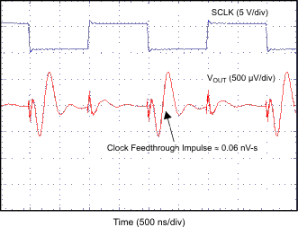
DAC7562 DAC7563 DAC8162 DAC8163 DAC8562 DAC8563 CLOCK_FEEDTHROUGH_5p5V.gif
Figure 48. Clock Feedthrough, 500 kHz, Midscale

7.7.3 Typical Characteristics: DAC at AVDD = 3.6 V

At TA = 25°C, 3.3-V external reference used, gain = 1 and DAC output not loaded, unless otherwise noted.
DAC7562 DAC7563 DAC8162 DAC8163 DAC8562 DAC8563 3p6V_POWER_SUPPLY_CURRENT_VS_TEMPERATURE_(DACs).png
Figure 49. Power-Supply Current vs Temperature
DAC7562 DAC7563 DAC8162 DAC8163 DAC8562 DAC8563 3p6V_IDD_VS_CODE_External_Ref.png
Figure 51. Power-Supply Current vs Digital Input Code
DAC7562 DAC7563 DAC8162 DAC8163 DAC8562 DAC8563 3p6V_IDD_EXTERNAL_REFERENCE_HISTOGRAM.gif
Figure 53. Power-Supply Current Histogram
DAC7562 DAC7563 DAC8162 DAC8163 DAC8562 DAC8563 3p6V_POWER_SUPPLY_CURRENT_VS_TEMPERATURE_(DACs_Reference).png
Figure 50. Power-Supply Current vs Temperature
DAC7562 DAC7563 DAC8162 DAC8163 DAC8562 DAC8563 3p6V_IDD_VS_CODE_Internal_Ref.png
Figure 52. Power-Supply Current vs Digital Input Code
DAC7562 DAC7563 DAC8162 DAC8163 DAC8562 DAC8563 3p6V_IDD_INTERNAL_REFERENCE_HISTOGRAM.gif
Figure 54. Power-Supply Current Histogram

7.7.4 Typical Characteristics: DAC at AVDD = 2.7 V

At TA = 25°C, 2.5-V external reference used, gain = 1, and DAC output not loaded, unless otherwise noted.
DAC7562 DAC7563 DAC8162 DAC8163 DAC8562 DAC8563 2p7V_LINEARITY_ERRORS_VS_DIGITAL_INPUT_CODE_COLD_(INL).png
Figure 55. Linearity Error vs Digital Input Code (–40°C)
DAC7562 DAC7563 DAC8162 DAC8163 DAC8562 DAC8563 2p7V_LINEARITY_ERRORS_VS_DIGITAL_INPUT_CODE_ROOM_(INL).png
Figure 57. Linearity Error vs Digital Input Code (25°C)
DAC7562 DAC7563 DAC8162 DAC8163 DAC8562 DAC8563 2p7V_LINEARITY_ERRORS_VS_DIGITAL_INPUT_CODE_HOT_(INL).png
Figure 59. Linearity Error vs Digital Input Code (125°C)
DAC7562 DAC7563 DAC8162 DAC8163 DAC8562 DAC8563 2p7V_LINEARITY_ERRORS_VS_TEMPERATURE_(INL).png
Figure 61. Linearity Error vs Temperature
DAC7562 DAC7563 DAC8162 DAC8163 DAC8562 DAC8563 2p7V_FULL_SCALE_ERROR_VS_TEMPERATURE.png
Figure 63. Full-Scale Error vs Temperature
DAC7562 DAC7563 DAC8162 DAC8163 DAC8562 DAC8563 2p7V_OFFSET_ERROR_VS_TEMPERATURE.png
Figure 65. Offset Error vs Temperature
DAC7562 DAC7563 DAC8162 DAC8163 DAC8562 DAC8563 2p7V_POWER_SUPPLY_CURRENT_VS_TEMPERATURE_(DACs).png
Figure 67. Power-Supply Current vs Temperature
DAC7562 DAC7563 DAC8162 DAC8163 DAC8562 DAC8563 2p7V_IDD_VS_CODE_External_Ref.png
Figure 69. Power-Supply Current vs Digital Input Code
DAC7562 DAC7563 DAC8162 DAC8163 DAC8562 DAC8563 2p7V_IDD_EXTERNAL_REFERENCE_HISTOGRAM.gif
Figure 71. Power-Supply Current Histogram
DAC7562 DAC7563 DAC8162 DAC8163 DAC8562 DAC8563 2p7V_POWER-DOWN_CURRENT_VS_TEMPERATURE_revC_si.png
Figure 73. Power-Down Current vs Temperature
DAC7562 DAC7563 DAC8162 DAC8163 DAC8562 DAC8563 FULL-SCALE_SETTLING_TIME_2p7V_RISING_EDGE.gif
Figure 75. Full-Scale Settling Time, Rising Edge
DAC7562 DAC7563 DAC8162 DAC8163 DAC8562 DAC8563 HALF-SCALE_SETTLING_TIME_2p7V_RISING_EDGE.gif
Figure 77. Half-Scale Settling Time, Rising Edge
DAC7562 DAC7563 DAC8162 DAC8163 DAC8562 DAC8563 GLITCH_ENERGY_2p7V_1_LSB_RISING_EDGE.gif
Figure 79. Glitch Impulse, Rising Edge, 1-LSB Step
DAC7562 DAC7563 DAC8162 DAC8163 DAC8562 DAC8563 GLITCH_ENERGY_2p7V_4_LSB_RISING_EDGE.gif
Figure 81. Glitch Impulse, Rising Edge, 4-LSB Step
DAC7562 DAC7563 DAC8162 DAC8163 DAC8562 DAC8563 GLITCH_ENERGY_2p7V_16_LSB_RISING_EDGE.gif
Figure 83. Glitch Impulse, Rising Edge, 16-LSB Step
DAC7562 DAC7563 DAC8162 DAC8163 DAC8562 DAC8563 POWER-ON_GLITCH_RESET_TO_ZERO_SCALE_2p7V.gif
Figure 85. Power-On Glitch, Reset to Zero Scale
DAC7562 DAC7563 DAC8162 DAC8163 DAC8562 DAC8563 CLOCK_FEEDTHROUGH_2p7V.gif
Figure 87. Clock Feedthrough, 500 kHz, Midscale
DAC7562 DAC7563 DAC8162 DAC8163 DAC8562 DAC8563 2p7V_LINEARITY_ERRORS_VS_DIGITAL_INPUT_CODE_COLD_(DNL).png
Figure 56. Differential Linearity Error vs Digital Input Code (–40°C)
DAC7562 DAC7563 DAC8162 DAC8163 DAC8562 DAC8563 2p7V_LINEARITY_ERRORS_VS_DIGITAL_INPUT_CODE_ROOM_(DNL).png
Figure 58. Differential Linearity Error vs Digital Input Code (25°C)
DAC7562 DAC7563 DAC8162 DAC8163 DAC8562 DAC8563 2p7V_LINEARITY_ERRORS_VS_DIGITAL_INPUT_CODE_HOT_(DNL).png
Figure 60. Differential Linearity Error vs Digital Input Code (125°C)
DAC7562 DAC7563 DAC8162 DAC8163 DAC8562 DAC8563 2p7V_LINEARITY_ERRORS_VS_TEMPERATURE_(DNL).png
Figure 62. Differential Linearity Error vs Temperature
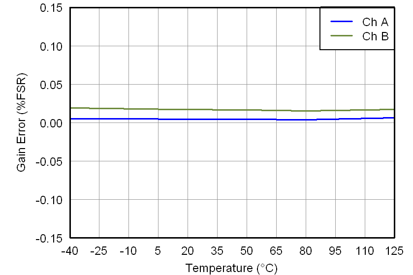
DAC7562 DAC7563 DAC8162 DAC8163 DAC8562 DAC8563 2p7V_GAIN_ERROR_VS_TEMPERATURE.png
Figure 64. Gain Error vs Temperature
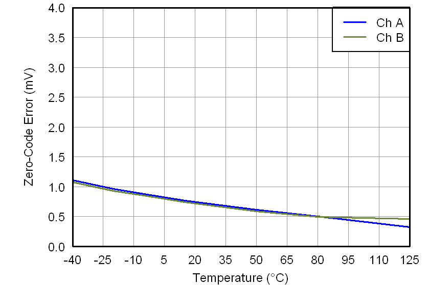
DAC7562 DAC7563 DAC8162 DAC8163 DAC8562 DAC8563 2p7V_ZERO_CODE_ERROR_VS_TEMPERATURE.png
Figure 66. Zero-Code Error vs Temperature
DAC7562 DAC7563 DAC8162 DAC8163 DAC8562 DAC8563 2p7V_POWER_SUPPLY_CURRENT_VS_TEMPERATURE_(DACs_Reference).png
Figure 68. Power-Supply Current vs Temperature
DAC7562 DAC7563 DAC8162 DAC8163 DAC8562 DAC8563 2p7V_IDD_VS_CODE_Internal_Ref.png
Figure 70. Power-Supply Current vs Digital Input Code
DAC7562 DAC7563 DAC8162 DAC8163 DAC8562 DAC8563 2p7V_IDD_INTERNAL_REFERENCE_HISTOGRAM.gif
Figure 72. Power-Supply Current Histogram
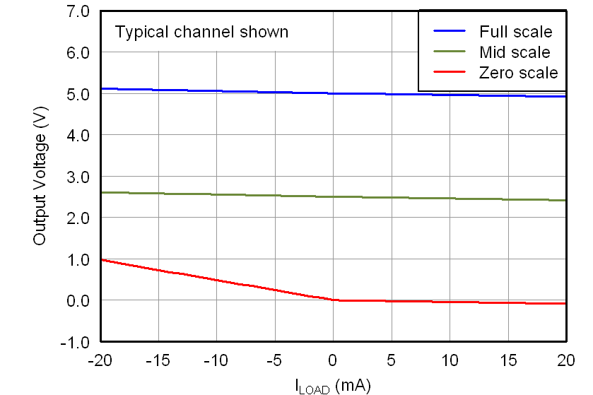
DAC7562 DAC7563 DAC8162 DAC8163 DAC8562 DAC8563 2p7V_DAC_LOAD_CURRENT.png
Figure 74. DAC Output Voltage vs Load Current
DAC7562 DAC7563 DAC8162 DAC8163 DAC8562 DAC8563 FULL-SCALE_SETTLING_TIME_2p7V_FALLING_EDGE.gif
Figure 76. Full-Scale Settling Time, Falling Edge
DAC7562 DAC7563 DAC8162 DAC8163 DAC8562 DAC8563 HALF-SCALE_SETTLING_TIME_2p7V_FALLING_EDGE.gif
Figure 78. Half-Scale Settling Time, Falling Edge
DAC7562 DAC7563 DAC8162 DAC8163 DAC8562 DAC8563 GLITCH_ENERGY_2p7V_1_LSB_FALLING_EDGE.gif
Figure 80. Glitch Impulse, Falling Edge, 1-LSB Step
DAC7562 DAC7563 DAC8162 DAC8163 DAC8562 DAC8563 GLITCH_ENERGY_2p7V_4_LSB_FALLING_EDGE.gif
Figure 82. Glitch Impulse, Falling Edge, 4-LSB Step
DAC7562 DAC7563 DAC8162 DAC8163 DAC8562 DAC8563 GLITCH_ENERGY_2p7V_16_LSB_FALLING_EDGE.gif
Figure 84. Glitch Impulse, Falling Edge, 16-LSB Step
DAC7562 DAC7563 DAC8162 DAC8163 DAC8562 DAC8563 POWER-ON_GLITCH_RESET_TO_MIDSCALE_2p7V.gif
Figure 86. Power-On Glitch, Reset to Midscale