SLASEE2 February 2018 DAC8771
PRODUCTION DATA.
- 1 Features
- 2 Applications
- 3 Description
- 4 Revision History
- 5 Device Comparison Table
- 6 Pin Configuration and Functions
- 7 Specifications
-
8 Detailed Description
- 8.1 Overview
- 8.2 Functional Block Diagram
- 8.3
Feature Description
- 8.3.1 Current Output Stage
- 8.3.2 Voltage Output Stage
- 8.3.3 Buck-Boost Converter
- 8.3.4 Analog Power Supply
- 8.3.5 Digital Power Supply
- 8.3.6 Internal Reference
- 8.3.7 Power-On-Reset
- 8.3.8 ALARM Pin
- 8.3.9 Power GOOD bit
- 8.3.10 Status Register
- 8.3.11 Status Mask
- 8.3.12 Alarm Action
- 8.3.13 Watchdog Timer
- 8.3.14 Programmable Slew Rate
- 8.3.15 HART Interface
- 8.4 Device Functional Modes
- 8.5
Register Maps
- 8.5.1
Register Maps
- 8.5.1.1 DAC8771 Commands
- 8.5.1.2
Register Maps and Bit Functions
- 8.5.1.2.1 No Operation Register (address = 0x00) [reset = 0x0000]
- 8.5.1.2.2 Reset Register (address = 0x01) [reset = 0x0000]
- 8.5.1.2.3 Reset Config Register (address = 0x02) [reset = 0x0000]
- 8.5.1.2.4 Select DAC Register (address = 0x03) [reset = 0x0000]
- 8.5.1.2.5 Configuration DAC Register (address = 0x04) [reset = 0x0000]
- 8.5.1.2.6 DAC Data Register (address = 0x05) [reset = 0x0000]
- 8.5.1.2.7 Select Buck-Boost Converter Register (address = 0x06) [reset = 0x0000]
- 8.5.1.2.8 Configuration Buck-Boost Register (address = 0x07) [reset = 0x0000]
- 8.5.1.2.9 DAC Channel Calibration Enable Register (address = 0x08) [reset = 0x0000]
- 8.5.1.2.10 DAC Channel Gain Calibration Register (address = 0x09) [reset = 0x0000]
- 8.5.1.2.11 DAC Channel Offset Calibration Register (address = 0x0A) [reset = 0x0000]
- 8.5.1.2.12 Status Register (address = 0x0B) [reset = 0x1000]
- 8.5.1.2.13 Status Mask Register (address = 0x0C) [reset = 0x0000]
- 8.5.1.2.14 Alarm Action Register (address = 0x0D) [reset = 0x0000]
- 8.5.1.2.15 User Alarm Code Register (address = 0x0E) [reset = 0x0000]
- 8.5.1.2.16 Reserved Register (address = 0x0F) [reset = N/A]
- 8.5.1.2.17 Write Watchdog Timer Register (address = 0x10) [reset = 0x0000]
- 8.5.1.2.18 Reserved Register (address 0x12 - 0xFF) [reset = N/A]
- 8.5.1
Register Maps
- 9 Application and Implementation
- 10Power Supply Recommendations
- 11Layout
- 12Device and Documentation Support
- 13Mechanical, Packaging, and Orderable Information
Package Options
Mechanical Data (Package|Pins)
- RGZ|48
Thermal pad, mechanical data (Package|Pins)
- RGZ|48
Orderable Information
7.7 Typical Characteristics
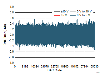 Figure 3. VOUT DNL vs Code (DC/DC Enabled)
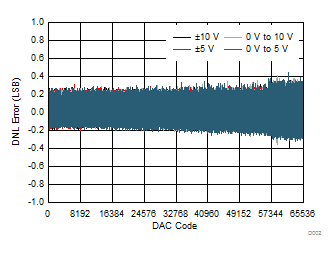 Figure 5. VOUT DNL vs Code (DC/DC Disabled)
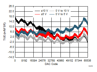 Figure 7. VOUT TUE vs Code (DC/DC Enabled)
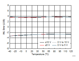 Figure 9. VOUT INL vs Temperature
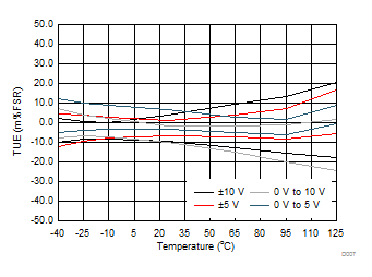 Figure 11. VOUT TUE vs Temperature
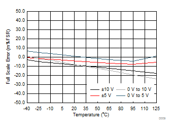 Figure 13. VOUT Full-Scale Error vs Temperature
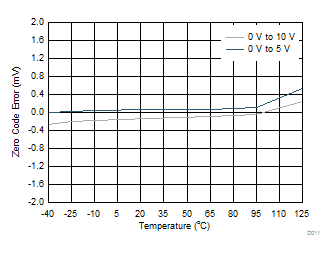 Figure 15. VOUT Zero-Code Error vs Temperature
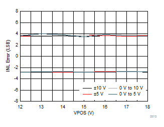 Figure 17. VOUT INL vs VPOS
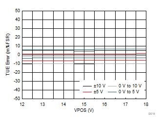 Figure 19. VOUT TUE vs VPOS
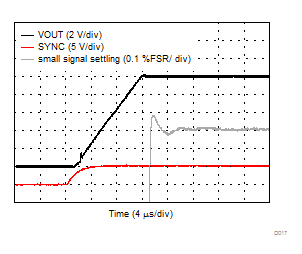 Figure 21. VOUT Settling Time, Rising Signal
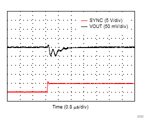 Figure 23. VOUT Major-Carry Glitch, Positive
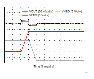 Figure 25. VOUT Power-On Glitch
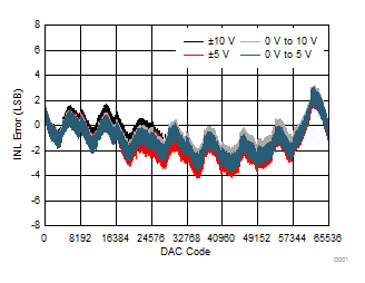 Figure 4. VOUT INL vs Code (DC/DC Enabled)
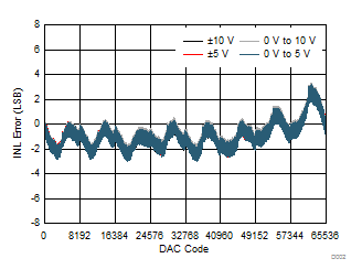 Figure 6. VOUT INL vs Code (DC/DC Disabled)
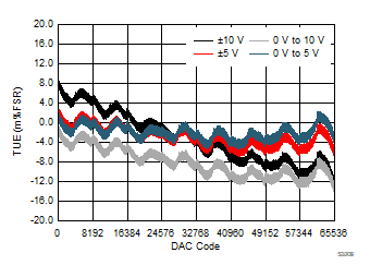 Figure 8. VOUT TUE vs Code (DC/DC Disabled)
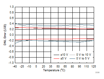 Figure 10. VOUT DNL vs Temperature
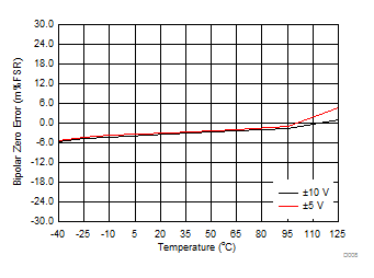 Figure 12. VOUT Bipolar Zero Error vs Temperature
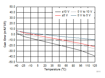 Figure 14. VOUT Gain Error vs Temperature
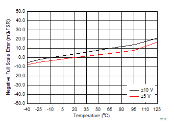 Figure 16. VOUT Negative Full-Scale Error vs Temperature
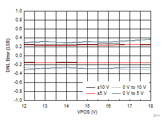 Figure 18. VOUT DNL vs VPOS
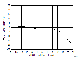 Figure 20. VOUT Load Regulation (SCLM = 11)
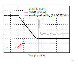 Figure 22. VOUT Settling Time, Falling Signal
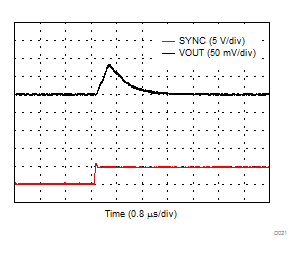 Figure 24. VOUT Major-Carry Glitch, Negative
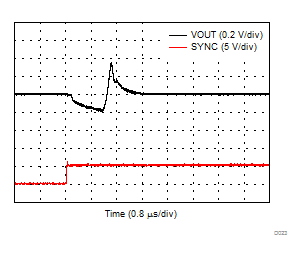 Figure 26. VOUT Output-Enable Glitch
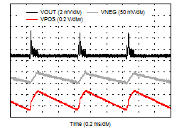 Figure 28. VOUT DC/DC Ripple (50kHz First-Order Low-Pass Filter)
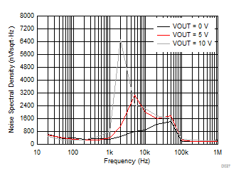 Figure 30. VOUT Noise Spectral Density (DC/DC Enabled)
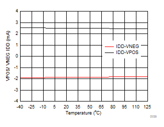 Figure 32. VOUT Quiescent Current vs Temperature (No Load)
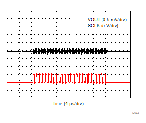 Figure 34. VOUT Digital Feedthrough
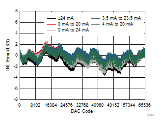 Figure 36. IOUT INL vs Code (DC/DC Enabled)
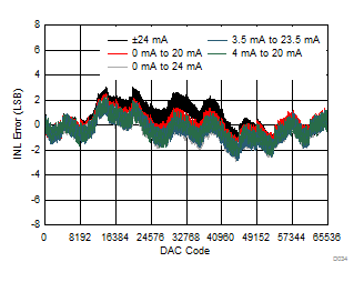 Figure 38. IOUT INL vs Code (DC/DC Disabled)
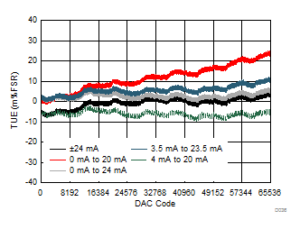 Figure 40. IOUT TUE vs Code (DC/DC Enabled)
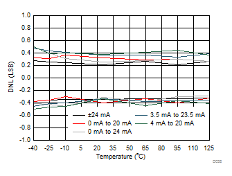 Figure 42. IOUT DNL vs Temperature
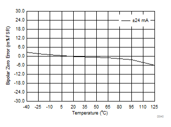 Figure 44. IOUT Bipolar Zero Error vs Temperature
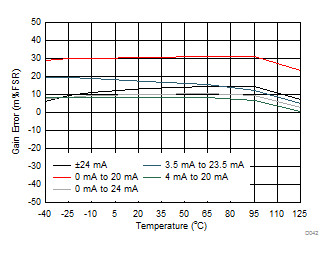 Figure 46. IOUT Gain Error vs Temperature
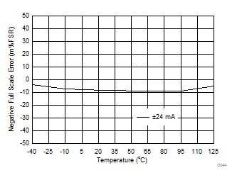 Figure 48. IOUT Negative Full-Scale Error vs Temperature
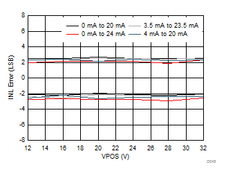 Figure 50. IOUT Unipolar Ranges INL vs VPOS
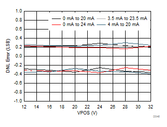 Figure 52. IOUT Unipolar Ranges DNL vs VPOS
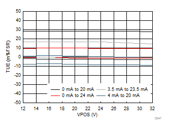 Figure 54. IOUT Unipolar Ranges TUE vs VPOS
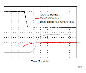 Figure 56. IOUT Settling Time, Falling Signal
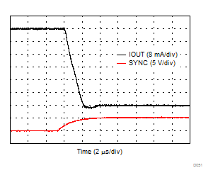 Figure 58. IOUT Settling Time, Bipolar Range, Falling Signal
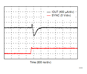 Figure 60. IOUT Major Carry Glitch, Negative
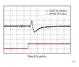 Figure 62. IOUT Output Enable Glitch
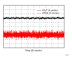 Figure 64. IOUT DC/DC Ripple (50kHz First-Order Low-Pass Filter)
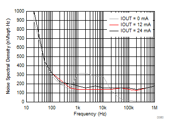 Figure 66. IOUT Noise Spectral Density (DC/DC Enabled)
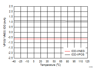 Figure 68. IOUT Quiescent Current vs Temperature
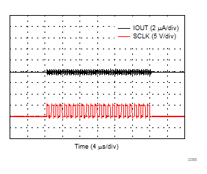 Figure 70. IOUT Digital Feed-Through
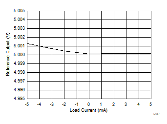 Figure 72. Internal Reference Voltage vs Load
 Figure 74. Internal Reference Voltage Noise Spectral Density (DC/DC Disabled)
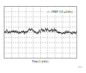 Figure 76. Internal Reference Voltage Noise (DC/DC Disabled)
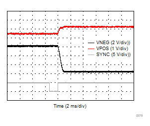 Figure 78. VPOS & VNEG Enable Settling Time
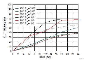 Figure 80. IOUT DC/DC Efficiency
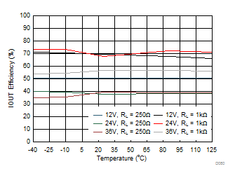 Figure 82. IOUT DC/DC Efficiency vs Temperature
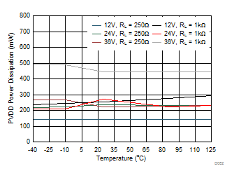 Figure 84. IOUT Power Dissipation vs Temperature
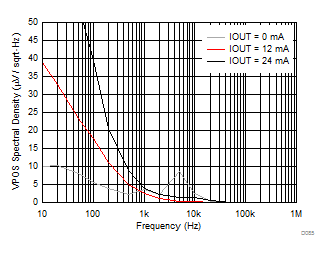 Figure 86. IOUT VPOS Noise Spectral Density
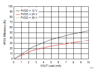 Figure 88. VOUT VPOS Efficiency vs Load
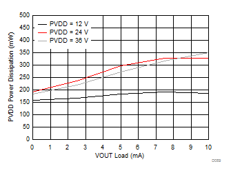 Figure 90. VOUT Power Dissipation vs Load
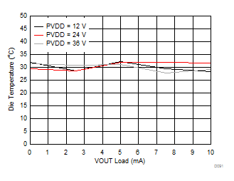 Figure 92. VOUT Die Temperature vs Load
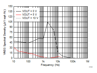 Figure 94. VPOS VNEG Noise Spectral Density
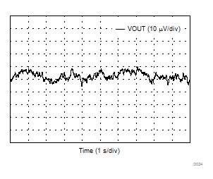 Figure 27. VOUT Noise (DC/DC Disabled)
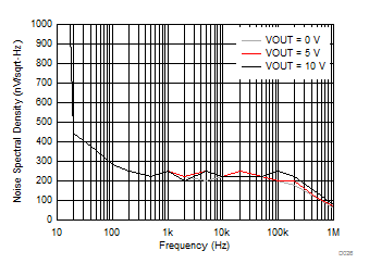 Figure 29. VOUT Noise Spectral Density (DC/DC Disabled)
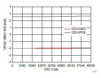 Figure 31. VOUT Quiescent Current vs Code (No Load)
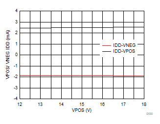 Figure 33. VOUT Quiescent Current vs VPOS (No Load)
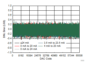 Figure 35. IOUT DNL vs Code (DC/DC Enabled)
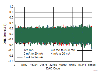 Figure 37. IOUT DNL vs Code (DC/DC Disabled)
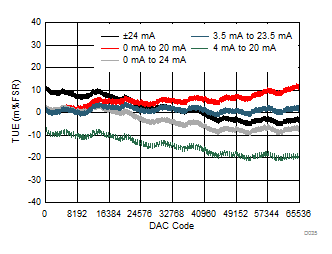 Figure 39. IOUT TUE vs Code (DC/DC Enabled)
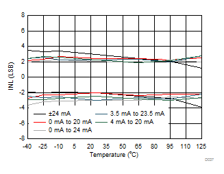 Figure 41. IOUT INL vs Temperature
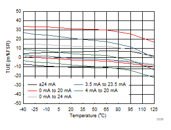 Figure 43. IOUT TUE vs Temperature
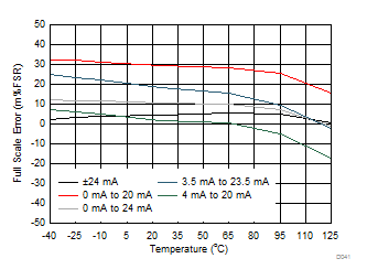 Figure 45. IOUT Full-Scale Error vs Temperature
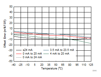 Figure 47. IOUT Offset Error vs Temperature
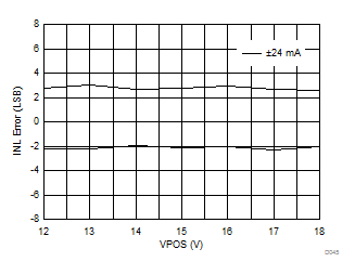 Figure 49. IOUT Bipolar Range INL vs VPOS
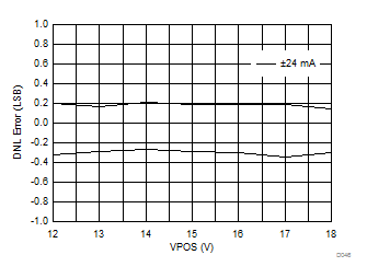 Figure 51. IOUT Bipolar Range DNL vs VPOS
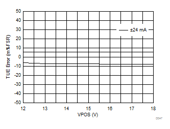 Figure 53. IOUT Bipolar Range TUE vs VPOS
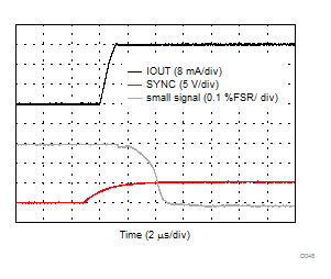 Figure 55. IOUT Settling Time, Rising Signal
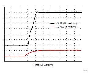 Figure 57. IOUT Settling Time, Bipolar Range, Rising Signal
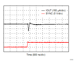 Figure 59. IOUT Major Carry Glitch, Positive
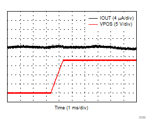 Figure 61. IOUT Power On Glitch
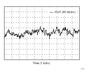 Figure 63. IOUT Noise (DC/DC Disabled)
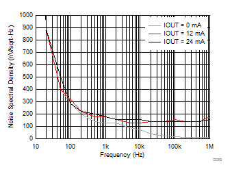 Figure 65. IOUT Noise Spectral Density (DC/DC Disabled)
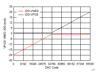 Figure 67. IOUT Quiescent Current vs Code, Bipolar Range
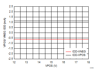 Figure 69. IOUT Quiescent Current vs VPOS
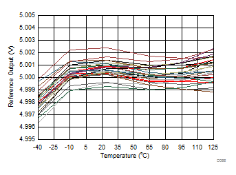 Figure 71. Internal Reference Voltage vs Temperature
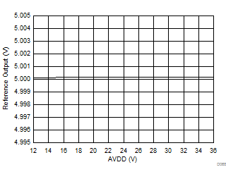 Figure 73. Internal Reference Voltage vs AVDD
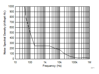 Figure 75. Internal Reference Voltage Noise Spectral Density (DC/DC Enabled)
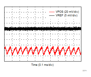 Figure 77. Internal Reference Voltage DC/DC Ripple
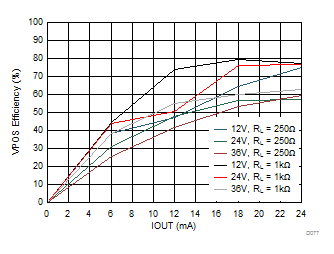 Figure 79. IOUT VPOS Efficiency
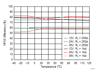 Figure 81. VPOS Efficiency vs Temperature
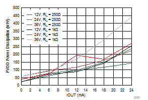 Figure 83. IOUT Power Dissipation vs Load
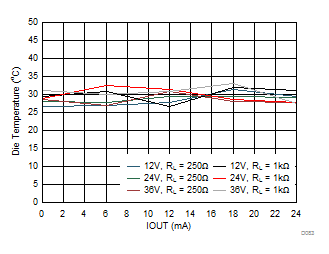 Figure 85. IOUT Die Temperature vs Load
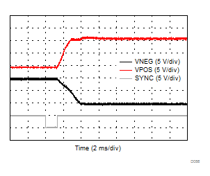 Figure 87. VOUT Enable VPOS and VNEG Settling Time
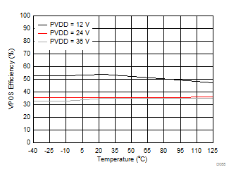 Figure 89. VOUT VPOS Efficiency vs Temperature
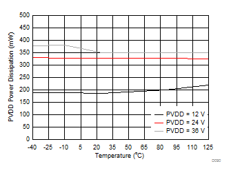 Figure 91. VOUT Power Dissipation vs Temperature
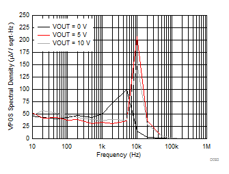 Figure 93. VOUT VPOS Noise Spectral Density
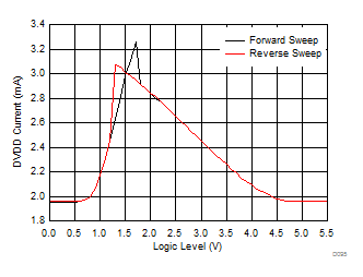 Figure 95. DVDD Iq vs Logic Level