SLASEE2 February 2018 DAC8771
PRODUCTION DATA.
- 1 Features
- 2 Applications
- 3 Description
- 4 Revision History
- 5 Device Comparison Table
- 6 Pin Configuration and Functions
- 7 Specifications
-
8 Detailed Description
- 8.1 Overview
- 8.2 Functional Block Diagram
- 8.3
Feature Description
- 8.3.1 Current Output Stage
- 8.3.2 Voltage Output Stage
- 8.3.3 Buck-Boost Converter
- 8.3.4 Analog Power Supply
- 8.3.5 Digital Power Supply
- 8.3.6 Internal Reference
- 8.3.7 Power-On-Reset
- 8.3.8 ALARM Pin
- 8.3.9 Power GOOD bit
- 8.3.10 Status Register
- 8.3.11 Status Mask
- 8.3.12 Alarm Action
- 8.3.13 Watchdog Timer
- 8.3.14 Programmable Slew Rate
- 8.3.15 HART Interface
- 8.4 Device Functional Modes
- 8.5
Register Maps
- 8.5.1
Register Maps
- 8.5.1.1 DAC8771 Commands
- 8.5.1.2
Register Maps and Bit Functions
- 8.5.1.2.1 No Operation Register (address = 0x00) [reset = 0x0000]
- 8.5.1.2.2 Reset Register (address = 0x01) [reset = 0x0000]
- 8.5.1.2.3 Reset Config Register (address = 0x02) [reset = 0x0000]
- 8.5.1.2.4 Select DAC Register (address = 0x03) [reset = 0x0000]
- 8.5.1.2.5 Configuration DAC Register (address = 0x04) [reset = 0x0000]
- 8.5.1.2.6 DAC Data Register (address = 0x05) [reset = 0x0000]
- 8.5.1.2.7 Select Buck-Boost Converter Register (address = 0x06) [reset = 0x0000]
- 8.5.1.2.8 Configuration Buck-Boost Register (address = 0x07) [reset = 0x0000]
- 8.5.1.2.9 DAC Channel Calibration Enable Register (address = 0x08) [reset = 0x0000]
- 8.5.1.2.10 DAC Channel Gain Calibration Register (address = 0x09) [reset = 0x0000]
- 8.5.1.2.11 DAC Channel Offset Calibration Register (address = 0x0A) [reset = 0x0000]
- 8.5.1.2.12 Status Register (address = 0x0B) [reset = 0x1000]
- 8.5.1.2.13 Status Mask Register (address = 0x0C) [reset = 0x0000]
- 8.5.1.2.14 Alarm Action Register (address = 0x0D) [reset = 0x0000]
- 8.5.1.2.15 User Alarm Code Register (address = 0x0E) [reset = 0x0000]
- 8.5.1.2.16 Reserved Register (address = 0x0F) [reset = N/A]
- 8.5.1.2.17 Write Watchdog Timer Register (address = 0x10) [reset = 0x0000]
- 8.5.1.2.18 Reserved Register (address 0x12 - 0xFF) [reset = N/A]
- 8.5.1
Register Maps
- 9 Application and Implementation
- 10Power Supply Recommendations
- 11Layout
- 12Device and Documentation Support
- 13Mechanical, Packaging, and Orderable Information
Package Options
Mechanical Data (Package|Pins)
- RGZ|48
Thermal pad, mechanical data (Package|Pins)
- RGZ|48
Orderable Information
8.3.2 Voltage Output Stage
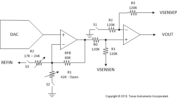
The voltage output stage as conceptualized in Figure 98 provides the voltage output according to the DAC code and the output range setting. The output range can be programmed as 0 V to +5 V or 0 V to +10 V for unipolar output mode, and ±5 V or ±10V for bipolar output mode. In addition, an option is available to increase the output voltage range by 20%. The output current drive can be up to 34 mA. The output stage has short-circuit current protection that limits the output current to 16 mA, this limit can be changed to 8 mA, 20 mA or 24 mA via writing bits 15 and 14 of address 0x04. The minimum headroom and foot-room for the voltage output stage is automatically maintained when the Buck-Boost converter is used to generate these supplies. However, when using an external supply for VPOS_IN and VNEG_IN pin (Buck-Boost converter disabled) the minimum headroom and foot-room as per must be maintained. In this case, the shows the maximum allowable difference between VPOS_IN and VNEG_IN.
The voltage output is designed to drive capacitive loads of up to 1 μF. For loads greater than 20 nF, an external compensation capacitor must be connected between CCOMP and VOUT to keep the output voltage stable at the expense of reduced bandwidth and increased settling time. Note that, a step response (due to input code change) on the voltage output pin loaded with large capacitive load (> 20 nF) triggers the short circuit limit circuit of the output stage. This results in setting the short circuit alarm status bits. Therefore, it is recommended to use slew rate control for large step change, when the voltage output pin is loaded with high capacitive loads.
 Figure 98. Voltage Output
The VSENSEP pin is provided to enable sensing of the load. Ideally, it is connected to VOUT at the terminals. Additionally, it can also be used to connect remotely to points electrically "nearer" to the load. This allows the internal output amplifier to ensure that the correct voltage is applied across the load as long as headroom is available on the power supply. However, if this line is cut, the amplifier loop would be broken. Therefore, an optional resistor can be used between VOUT and VSENSEP to prevent this.
The VSENSEN pin can be used to sense the remote ground and offset the VOUT pin accordingly. The VSENSEN pin can sense a maximum of ±7 V difference from the GND pin of the DAC8771.
The 16 bit data can be written to DAC8771 as shown in DAC data registers,Table 4 and Table 5.
For unipolar output mode:

For bipolar output mode:

Where:
- CODE is the decimal equivalent of the code loaded to the DAC.
- N is the bits of resolution; 16
- VREFIN is the reference voltage; for internal reference, VREFIN = +5 V.
- GAIN is automatically selected for a desired voltage output range as shown in