SBAS349F August 2005 – June 2016 DAC8812
PRODUCTION DATA.
- 1 Features
- 2 Applications
- 3 Description
- 4 Revision History
- 5 Device Comparison Table
- 6 Pin Configuration and Functions
- 7 Specifications
- 8 Detailed Description
- 9 Application and Implementation
- 10Power Supply Recommendations
- 11Layout
- 12Device and Documentation Support
- 13Mechanical, Packaging, and Orderable Information
Package Options
Mechanical Data (Package|Pins)
- PW|16
Thermal pad, mechanical data (Package|Pins)
Orderable Information
7 Specifications
7.1 Absolute Maximum Ratings
over operating ambient temperature range (unless otherwise noted)(1)(1) Stresses beyond those listed under Absolute Maximum Ratings may cause permanent damage to the device. These are stress ratings only, which do not imply functional operation of the device at these or any other conditions beyond those indicated under Recommended Operating Conditions. Exposure to absolute-maximum-rated conditions for extended periods may affect device reliability.
7.2 ESD Ratings
| VALUE | UNIT | |||
|---|---|---|---|---|
| V(ESD) | Electrostatic discharge | Human-body model (HBM), per ANSI/ESDA/JEDEC JS-001(1) | ±4000 | V |
| Charged-device model (CDM), per JEDEC specification JESD22-C101(2) | ±1000 | |||
(1) JEDEC document JEP155 states that 500-V HBM allows safe manufacturing with a standard ESD control process. Pins listed as ±4000 V may actually have higher performance.
(2) JEDEC document JEP157 states that 250-V CDM allows safe manufacturing with a standard ESD control process. Pins listed as ±1000 V may actually have higher performance.
7.3 Recommended Operating Conditions
over operating ambient temperature range (unless otherwise noted)| MIN | NOM | MAX | UNIT | ||
|---|---|---|---|---|---|
| VDD | Supply voltage to GND | 2.7 | 5.5 | V | |
| TA | Operating ambient temperature | –40 | 85 | °C | |
7.4 Thermal Information
| THERMAL METRIC(1) | DAC8812 | UNIT | |
|---|---|---|---|
| PW (TSSOP) | |||
| 16 PINS | |||
| RθJA | Junction-to-ambient thermal resistance | 100.6 | °C/W |
| RθJC(top) | Junction-to-case (top) thermal resistance | 32.8 | °C/W |
| RθJB | Junction-to-board thermal resistance | 46.8 | °C/W |
| ψJT | Junction-to-top characterization parameter | 2 | °C/W |
| ψJB | Junction-to-board characterization parameter | 46 | °C/W |
(1) For more information about traditional and new thermal metrics, see the Semiconductor and IC Package Thermal Metrics application report, SPRA953.
7.5 Electrical Characteristics
VDD = 2.7 V to 5.5 V, IOUTX = Virtual GND, AGNDX = 0 V, VREFA,B = 10 V, TA = full operating temperature range, unless otherwise noted.| PARAMETER | CONDITIONS | MIN | TYP | MAX | UNIT | |
|---|---|---|---|---|---|---|
| STATIC PERFORMANCE(1) | ||||||
| Resolution | 16 | Bits | ||||
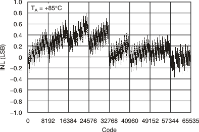
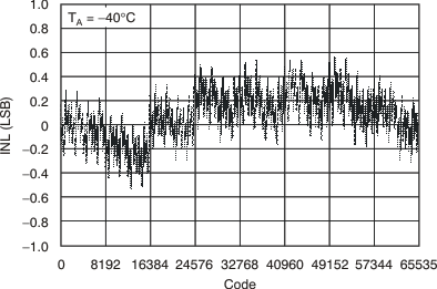
| INL | Relative accuracy | DAC8812B | ±2 | LSB | ||
| DAC8812C | ±1 | |||||
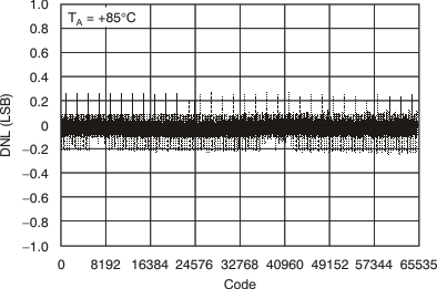
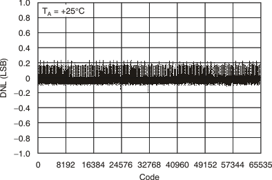
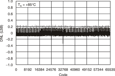
| DNL | Differential nonlinearity | ±1 | LSB | |||
| IOUTx | Output leakage current | Data = 0000h, TA = 25°C | 10 | nA | ||
| Data = 0000h, TA = TA max | 20 | |||||
| GFSE | Full-scale gain error | Data = FFFFh | ±0.75 | ±4 | mV | |
| TCVFS | Full-scale temperature coefficient(2) | 1 | ppm/°C | |||
| RFBX | Feedback resistor | VDD = 5 V | 5 | kΩ | ||
| REFERENCE INPUT(2) | ||||||
| VREFx | VREFx range | –15 | 15 | V | ||
| RREFx | Input resistance | 4 | 5 | 6 | kΩ | |
| Channel-to-channel input resistance match | 1% | |||||
| CREFx | Input capacitance | 5 | pF | |||
| ANALOG OUTPUT(2) | ||||||
| IOUTx | Output current | Data = FFFFh | 1.6 | 2.5 | mA | |
| COUTx | Output capacitance | Code-dependent | 50 | pF | ||
| LOGIC INPUTS(2) | ||||||
| VIL | Input low voltage | VDD = 2.7 V | 0.6 | V | ||
| VDD = 5 V | 0.8 | |||||
| VIH | Input high voltage | VDD = 2.7 V | 2.1 | V | ||
| VDD = 5 V | 2.4 | |||||
| IIL | Input leakage current | 1 | μA | |||
| CIL | Input capacitance | 10 | pF | |||
| SUPPLY CHARACTERISTICS | ||||||
| VDD RANGE | Power supply range | 2.7 | 5.5 | V | ||
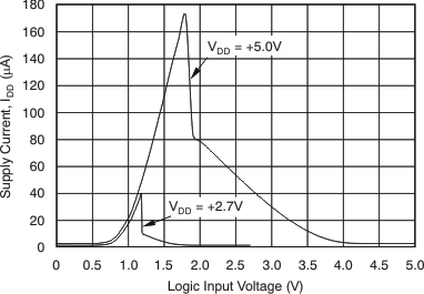
| IDD | Positive supply current | Logic inputs = 0 V, VDD = 4.5 V to 5.5 V | 2 | 5 | μA | |
| Logic inputs = 0 V, VDD = 2.7 V to 3.6 V | 1 | 2.5 | μA | |||
| PDISS | Power dissipation | Logic inputs = 0 V | 0.0275 | mW | ||
| PSS | Power supply sensitivity | ΔVDD = ±5% | 0.006% | |||
| AC CHARACTERISTICS(2) (3) | ||||||
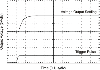
| ts | Output voltage settling time | To ±0.1% of full-scale, Data = 0000h to FFFFh to 0000h |
0.3 | µs | ||
| To ±0.0015% of full-scale, Data = 0000h to FFFFh to 0000h |
0.5 | |||||
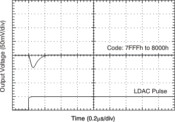
| QG | DAC glitch impulse | Data = 7FFFh to 8000h to 7FFFh | 5 | nV-s | ||
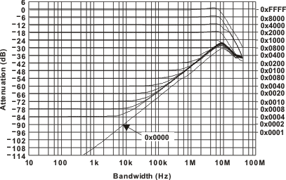
| BW –3 dB | Reference multiplying BW | VREFx = 100 mVRMS, Data = FFFFh, CFB = 3 pF | 10 | MHz | ||
| Feedthrough error | Data = 0000h, VREFx = 100 mVRMS, f = 100 kHz | –70 | dB | |||
| Crosstalk error | Data = 0000h, VREFB = 100 mVRMS, Adjacent channel, f = 100 kHz |
–100 | dB | |||
| QD | Digital feedthrough | CS = 1 and fCLK = 1 MHz | 1 | nV-s | ||
| THD | Total harmonic distortion | VREF = 5 VPP, Data = FFFFh, f = 1 kHz | –105 | dB | ||
| en | Output spot noise voltage | f = 1 kHz, BW = 1 Hz | 12 | nV/√Hz | ||
(1) All static performance tests (except IOUT) are performed in a closed-loop system using an external precision OPA277 I-to-V converter amplifier. The DAC8812 RFB pin is tied to the amplifier output. Typical values represent average readings measured at 25°C.
(2) These parameters are not subject to production testing.
(3) All ac characteristic tests are performed in a closed-loop system using a THS4011 I-to-V converter amplifier.
7.6 Timing Requirements
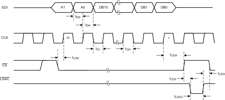
See Figure 1| MIN | NOM | MAX | UNIT | ||
|---|---|---|---|---|---|
| INTERFACE TIMING(1) | |||||
| tCH | Clock duration, high | 10 | ns | ||
| tCL | Clock duration, low | 10 | ns | ||
| tCSS | CS to clock setup | 0 | ns | ||
| tCSH | Clock to CS hold | 10 | ns | ||
| tLDAC | Load DAC pulse duration | 20 | ns | ||
| tDS | Data setup | 10 | ns | ||
| tDH | Data hold | 10 | ns | ||
| tLDS | Load setup | 5 | ns | ||
| tLDH | Load hold | 25 | ns | ||
(1) All input control signals are specified with tR = tF = 2.5 ns (10% to 90% of 3 V) and timed from a voltage level of 1.5 V.
7.7 Switching Characteristics
over operating ambient temperature range (unless otherwise noted)| PARAMETER | TEST CONDITIONS | MIN | TYP | MAX | UNIT | |
|---|---|---|---|---|---|---|
| INTERFACE TIMING | ||||||
| tPD | Clock to SDO propagation delay | 2 | 20 | ns | ||
7.8 Typical Characteristics
7.8.1 Channel A—5 V
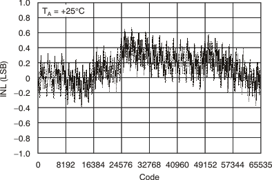
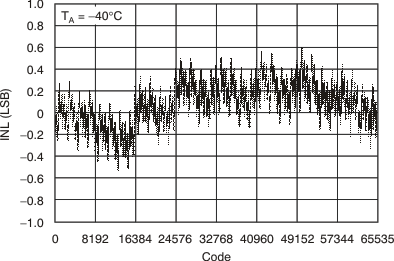
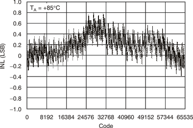
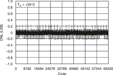
At TA = 25°C, VDD = 5 V, unless otherwise noted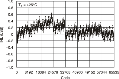


7.8.2 Channel B—5 V
At TA = 25°C, VDD = 5 V, unless otherwise noted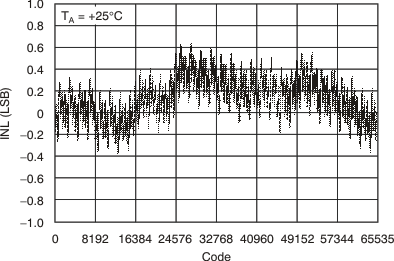
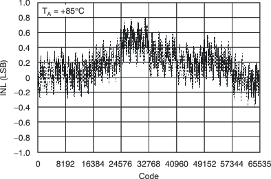
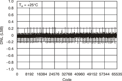
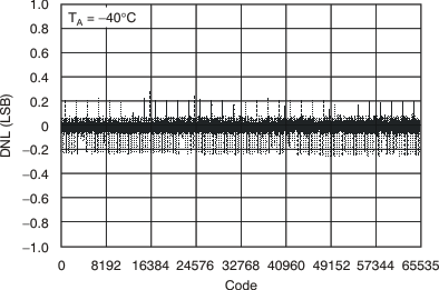
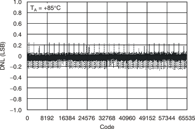
7.8.3 Channel A and B—5 V
At TA = 25°C, VDD = 5 V, unless otherwise noted7.8.4 Channel A—2.7 V
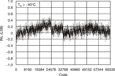
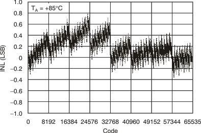
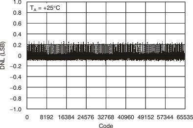
At TA = 25°C, VDD = 2.7 V, unless otherwise noted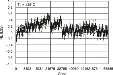
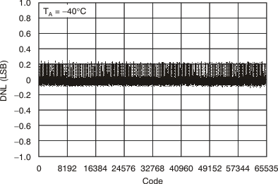
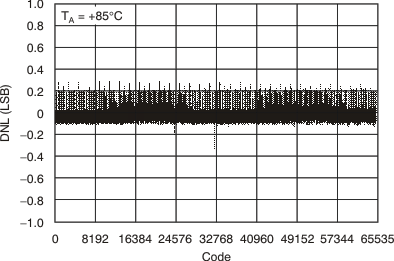
7.8.5 Channel B—2.7 V
At TA = 25°C, VDD = 2.7 V, unless otherwise noted