SBVS012I December   2000  – September 2020 DCP010505B , DCP010505DB , DCP010507DB , DCP010512B , DCP010512DB , DCP010515B , DCP010515DB , DCP011512DB , DCP011515DB , DCP012405B , DCP012415DB

PRODUCTION DATA  

  1. Features
  2. Applications
  3. Description
  4. Revision History
  5. Pin Configuration and Functions
    1.     Pin Functions
  6. Specifications
    1. 6.1 Absolute Maximum Ratings
    2. 6.2 ESD Ratings
    3. 6.3 Recommended Operating Conditions
    4. 6.4 Thermal Information
    5. 6.5 Electrical Characteristics
    6. 6.6 Switching Characteristics
    7. 6.7 Typical Characteristics
  7. Detailed Description
    1. 7.1 Overview
    2. 7.2 Functional Block Diagrams
    3. 7.3 Feature Description
      1. 7.3.1  Isolation
        1. 7.3.1.1 Operation or Functional Isolation
        2. 7.3.1.2 Basic or Enhanced Isolation
        3. 7.3.1.3 Continuous Voltage
        4. 7.3.1.4 Isolation Voltage
        5. 7.3.1.5 Repeated High-Voltage Isolation Testing
      2. 7.3.2  Power Stage
      3. 7.3.3  Oscillator And Watchdog Circuit
      4. 7.3.4  Thermal Shutdown
      5. 7.3.5  Synchronization
      6. 7.3.6  Light Load Operation (< 10%)
      7. 7.3.7  Load Regulation (10% to 100%)
      8. 7.3.8  Construction
      9. 7.3.9  Thermal Management
      10. 7.3.10 Power-Up Characteristics
    4. 7.4 Device Functional Modes
      1. 7.4.1 Disable and Enable (SYNCIN Pin)
      2. 7.4.2 Decoupling
        1. 7.4.2.1 Ripple Reduction
        2. 7.4.2.2 Connecting the DCP01B in Series
        3. 7.4.2.3 Connecting the DCP01B in Parallel
  8. Application and Implementation
    1. 8.1 Application Information
    2. 8.2 Typical Application
      1. 8.2.1 Design Requirements
      2. 8.2.2 Detailed Design Procedure
        1. 8.2.2.1 Input Capacitor
        2. 8.2.2.2 Output Capacitor
        3. 8.2.2.3 SYNCIN Pin
      3. 8.2.3 DCP010505 Application Curves
      4. 8.2.4 PCB Design
      5. 8.2.5 Decoupling Ceramic Capacitors
      6. 8.2.6 Input Capacitor and the Effects of ESR
      7. 8.2.7 Ripple and Noise
        1. 8.2.7.1 Output Ripple Calculation Example
      8. 8.2.8 Dual DCP01B Output Voltage
      9. 8.2.9 Optimizing Performance
  9. Power Supply Recommendations
  10. 10Layout
    1. 10.1 Layout Guidelines
    2. 10.2 Layout Example
  11. 11Device and Documentation Support
    1. 11.1 Device Support
      1. 11.1.1 Device Nomenclature
    2. 11.2 Documentation Support
      1. 11.2.1 Related Documentation
    3. 11.3 Receiving Notification of Documentation Updates
    4. 11.4 Support Resources
    5. 11.5 Trademarks
    6. 11.6 Glossary
    7. 11.7 Electrostatic Discharge Caution
  12. 12Mechanical, Packaging, and Orderable Information

Package Options

Mechanical Data (Package|Pins)
Thermal pad, mechanical data (Package|Pins)
Orderable Information

Connecting the DCP01B in Parallel

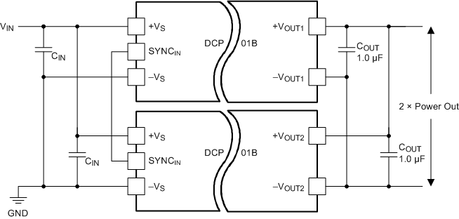
If the output power from one DCP01B is not sufficient, it is possible to parallel the outputs of multiple DCP01Bs, as shown in Figure 7-8 (applies to single output devices only). The synchronization feature allows easy synchronization to prevent power-rail beat frequencies at no additional filtering cost.
GUID-BD37B335-CBA4-4FE0-A438-293142442545-low.gifFigure 7-8 Multiple DCP01B Devices Connected in Parallel