SBVS013E October 2001 – July 2022 DCR010503 , DCR010505 , DCR011203 , DCR011205 , DCR012403 , DCR012405
PRODUCTION DATA
- 1 Features
- 2 Applications
- 3 Description
- 4 Revision History
- 5 Device Comparison Table
- 6 Pin Configuration and Functions
- 7 Specifications
-
8 Detailed Description
- 8.1 Overview
- 8.2 Functional Block Diagram
- 8.3 Feature Description
- 8.4 Device Functional Modes
- 9 Application and Implementation
- 10Power Supply Recommendations
- 11Layout
- 12Device and Documentation Support
- 13Mechanical, Packaging, and Orderable Information
Package Options
Mechanical Data (Package|Pins)
Thermal pad, mechanical data (Package|Pins)
Orderable Information
3 Description
The DCR01 family is a series of high-efficiency, input-isolated, output-regulated DC/DC converters. In addition to 1-W nominal, galvanically-isolated output power capability, this range of DC/DC converters offer very low output noise, thermal protection, and high accuracy.
This combination of features and small size makes the DCR01 series of devices suitable for a wide range of applications, and is an easy-to-use solution in applications requiring signal path isolation.
CAUTION: This product has
operational isolation and is intended for signal isolation only. It must not be used
as a part of a safety isolation circuit requiring reinforced isolation. See
definitions in the feature description.
Device
Information
| Part Number | Package(1) | Body Size (NOM) |
|---|---|---|
| DCR01 | PDIP (10) | 22.86 mm × 6.61 mm |
| SOP (12) | 17.90 mm × 7.50 mm |
(1) For all available packages, see the orderable addendum at the end of the data sheet.
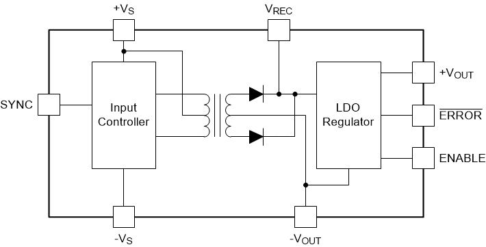
 DCR01 Block Diagram