SBVS013E October   2001  – July 2022 DCR010503 , DCR010505 , DCR011203 , DCR011205 , DCR012403 , DCR012405

PRODUCTION DATA  

  1. Features
  2. Applications
  3. Description
  4. Revision History
  5. Device Comparison Table
  6. Pin Configuration and Functions
  7. Specifications
    1. 7.1 Absolute Maximum Ratings
    2. 7.2 ESD Ratings
    3. 7.3 Recommended Operating Conditions
    4. 7.4 Thermal Information
    5. 7.5 Electrical Characteristics
    6. 7.6 Typical Characteristics
  8. Detailed Description
    1. 8.1 Overview
    2. 8.2 Functional Block Diagram
    3. 8.3 Feature Description
      1. 8.3.1  Isolation
        1. 8.3.1.1 Operation or Functional Isolation
        2. 8.3.1.2 Basic or Enhanced Isolation
        3. 8.3.1.3 Working Voltage
        4. 8.3.1.4 Isolation Voltage Rating
        5. 8.3.1.5 Repeated High-Voltage Isolation Testing
      2. 8.3.2  Power Stage
      3. 8.3.3  Rectification
      4. 8.3.4  Regulator
      5. 8.3.5  Oscillator and Watchdog
      6. 8.3.6  ERROR Flag
      7. 8.3.7  Synchronization
      8. 8.3.8  Construction
      9. 8.3.9  Thermal Considerations
      10. 8.3.10 Decoupling – Ripple Reduction
    4. 8.4 Device Functional Modes
      1. 8.4.1 Device Disable and Enable
      2. 8.4.2 Regulated Output Disable and Enable
  9. Application and Implementation
    1. 9.1 Application Information
      1. 9.1.1 DCR01 Single Voltage Output
      2. 9.1.2 Generating Two Positive Output Voltages
      3. 9.1.3 Generation of Dual Polarity Voltages from Two Self-Synchronized DCR01s
    2. 9.2 Typical Application
      1. 9.2.1 Design Requirements
      2. 9.2.2 Detailed Design Procedure
        1. 9.2.2.1 Input Capacitor
        2. 9.2.2.2 Output Capacitor
        3. 9.2.2.3 Filter Capacitor
        4. 9.2.2.4 ERROR Flag
      3. 9.2.3 Application Curves
  10. 10Power Supply Recommendations
  11. 11Layout
    1. 11.1 Layout Guidelines
    2. 11.2 Layout Examples
  12. 12Device and Documentation Support
    1. 12.1 Receiving Notification of Documentation Updates
    2. 12.2 Support Resources
    3. 12.3 Trademarks
    4. 12.4 Electrostatic Discharge Caution
    5. 12.5 Glossary
  13. 13Mechanical, Packaging, and Orderable Information

Package Options

Mechanical Data (Package|Pins)
Thermal pad, mechanical data (Package|Pins)
Orderable Information

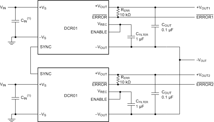
Generating Two Positive Output Voltages

Two DCR01s can be used to create output voltages of +3.3 V and +5 V, as shown in Figure 9-2. The two DCR01s are connected in self-synchronization, thus locking the oscillators of both devices to a single frequency. The ERROR and ENABLE facilities can be used in a similar configuration for a single DCR01. The filter capacitors connected to the VREC pins (CFILTER) must be kept separate from each other and connected in close proximity to their respective DCR01.
GUID-E456B1C0-9AC7-41AA-BD73-ADBF36C7D4D8-low.gif
CIN = 2.2 μF for 5-V input devices and 0.47 μF for 12-V and 24-V input devices. Low-ESR, ceramic capacitors are required.
Figure 9-2 Two Positive Voltages from Self-Synchronized DCR01s