SBVS014C August 2000 – August 2021 DCV010505 , DCV010505D , DCV010512 , DCV010512D , DCV010515 , DCV010515D , DCV011512D , DCV011515D , DCV012405 , DCV012415D
PRODUCTION DATA
- 1 Features
- 2 Applications
- 3 Description
- 4 Revision History
- 5 Device Comparison Table
- 6 Pin Configuration and Functions
- 7 Specifications
-
8 Detailed Description
- 8.1 Overview
- 8.2 Functional Block Diagrams
- 8.3 Feature Description
- 8.4 Device Functional Modes
-
9 Application and Implementation
- 9.1 Application Information
- 9.2
Typical Application
- 9.2.1 Design Requirements
- 9.2.2 Detailed Design Procedure
- 9.2.3 Application Curves
- 10Power Supply Recommendations
- 11Layout
- 12Device and Documentation Support
- 13Mechanical, Packaging, and Orderable Information
Package Options
Mechanical Data (Package|Pins)
Thermal pad, mechanical data (Package|Pins)
Orderable Information
6 Pin Configuration and Functions
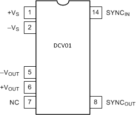
 Figure 6-1 NVA, DUA Package7-Pin PDIP, SOP (Single-Output)(Top View)
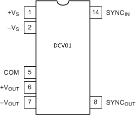
 Figure 6-2 NVA, DUA Package7-Pin PDIP, SOP (Dual-Output)
(Top View)
Figure 6-2 NVA, DUA Package7-Pin PDIP, SOP (Dual-Output)
(Top View)Table 6-1 Pin Functions
| PIN | I/O | DESCRIPTION | ||
|---|---|---|---|---|
| NAME | SINGLE-OUTPUT | DUAL-OUTPUT | ||
| COM | — | 5 | O | Output side common |
| NC | 7 | — | — | No connection |
| SYNCIN | 14 | 14 | I | Synchronization. Synchronize multiple devices by connecting the SYNC pins of each. Pulling this pin low disables the internal oscillator. |
| SYNCOUT | 8 | 8 | O | Synchronization output. Unrectified transformer output |
| +VOUT | 6 | 6 | O | Positive output voltage |
| +VS | 1 | 1 | I | Input voltage |
| –VOUT | 5 | 7 | O | Negative output voltage |
| –VS | 2 | 2 | I | Input side common |