-
DDC264 64-Channel, Current-Input Analog-to-Digital Converter
- 1 Features
- 2 Applications
- 3 Description
- 4 Revision History
- 5 Device Comparison Table
- 6 Pin Configuration and Functions
- 7 Specifications
-
8 Detailed Description
- 8.1 Overview
- 8.2 Functional Block Diagram
- 8.3
Feature Description
- 8.3.1 Dual Switched Integrator: Basic Integration Cycle
- 8.3.2 Integration Capacitors
- 8.3.3 Voltage Reference
- 8.3.4 Serial Data Output and Control Interface
- 8.4 Device Functional Modes
- 8.5 Programming
- 8.6 Register Maps
- 9 Application and Implementation
- 10Power Supply Recommendations
- 11Layout
- 12Device and Documentation Support
- 13Mechanical, Packaging, and Orderable Information
- IMPORTANT NOTICE
Package Options
Mechanical Data (Package|Pins)
- ZAW|100
Thermal pad, mechanical data (Package|Pins)
Orderable Information
DDC264 64-Channel, Current-Input Analog-to-Digital Converter
1 Features
- Single-Chip Solution to Directly Measure 64 Low-Level Currents
- Proven High-Precision, True Integrating Architecture With 100% Charge Collection
- Easy Upgrade for Existing DDC Family Applications
- Very Low Power: 3 mW/channel
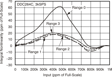
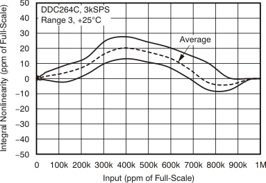
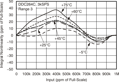
- Extremely Linear:
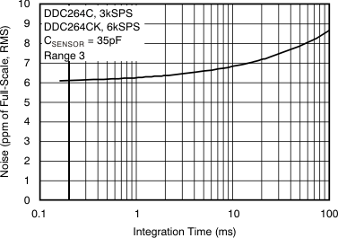
INL = ±0.025% of Reading ±1 ppm of FSR - Low Noise: 6.3 ppm of FSR
- Adjustable Full-Scale Range
- Adjustable Speed
- Data Rates up to 6 kSPS With 20-bit Performance
- Integration Times as low as 160 µs
- Daisy-Chainable Serial Interface
- In-Package Bypass Capacitors Simplify PCB Design
2 Applications
- CT Scanner DAS
- Photodiode Sensors
- X-Ray Detection Systems
SPACER
SPACER
Simplified Schematic
3 Description
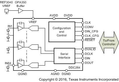
The DDC264 is a 20-bit, 64-channel, current-input analog-to-digital (A/D) converter. It combines both current-to-voltage and A/D conversion so that 64 separate low-level current output devices, such as photodiodes, can be directly connected to its inputs and digitized.
For each of the 64 inputs, the DDC264 uses the proven dual switched integrator front-end. This configuration allows for continuous current integration: while one integrator is being digitized by the onboard A/D converter, the other is integrating the input current. This architecture provides both a very stable offset and a loss-less collection of the input current. Adjustable integration times range from 160 µs to 1 s, allowing currents from fAs to µAs to be continuously measured with outstanding precision.
The DDC264 has a serial interface designed for daisy-chaining in multi-device systems. Simply connect the output of one device to the input of the next to create the chain. Common clocking feeds all the devices in the chain so that the digital overhead in a multi-DDC264 system is minimal.
The DDC264 uses a 5-V analog supply and a 2.7-V to 3.6-V digital supply. Bypass capacitors within the DDC264 package help minimize the external component requirements. Operating over the temperature range of 0°C to 70°C, the DDC264
100-pin NFBGA package is offered in two versions: the DDC264C for low-power applications, and the DDC264CK when higher speeds are required.
Device Information(1)
| PART NUMBER | PACKAGE | BODY SIZE (NOM) |
|---|---|---|
| DDC264 | NFBGA (100) | 9.00 mm × 9.00 mm |
- For all available packages, see the orderable addendum at the end of the data sheet.
4 Revision History
Changes from C Revision (July 2011) to D Revision
- Added ESD Ratings table, Feature Description section, Device Functional Modes, Application and Implementation section, Power Supply Recommendations section, Layout section, Device and Documentation Support section, and Mechanical, Packaging, and Orderable Information sectionGo
- Moved AVDD and DVDD rows to Recommended Operating Conditions tableGo
- Moved Dynamic Characteristics rows to Recommended Operating Conditions table Go
- Deleted Voltage row from Electrical Characteristics table Go
- Changed 1.65 mA to 825 µA in Voltage Reference sectionGo
- Changed 680 µA to 340 µA in Voltage Reference sectionGo
- Changed 64 to 128 in the formula in Reading the Measurement sectionGo
- Changed high-impedance to low-impedance in Shielding Analog Signal Paths sectionGo
Changes from B Revision (January, 2011) to C Revision
- Updated NOISE vs CSENSOR table; revised values for Range 0 performance in fC and ElectronsGo
Changes from A Revision (January, 2011) to B Revision
- Changed second paragraph of Basic Integration Cycle section to correct CONV timing description errorGo
5 Device Comparison Table
| PRODUCT | NO. OF CHANNELS | FULL-SCALE | MAXIMUM DATA RATE |
POWER/CHANNEL AT MAX DATA RATE |
PACKAGE-PIN |
|---|---|---|---|---|---|
| DDC112 | 2 | 1000 pC | 2 KSPS | 80 mW | SO-28, TQFP-32 |
| DDC112K | 2 | 1000 pC | 3 KSPS | 85 mW | SO-28, TQFP-32 |
| DDC114 | 4 | 350 pC | 3.1 KSPS | 18 mW | QFN-48 |
| DDC118 | 8 | 350 pC | 3.1 KSPS | 18 mW | QFN-48 |
| DDC316 | 16 | 12 pC | 100 KSPS | 28 mW | BGA-64 |
| DDC232C | 32 | 350 pC | 3.1 KSPS | 7 mW | BGA-64 |
| DDC232CK | 32 | 350 pC | 6.2 KSPS | 10 mW | BGA-64 |
| DDC264C | 64 | 150 pC | 3.1 KSPS | 3 mW | BGA-100 |
| DDC264CK | 64 | 150 pC | 6.2 KSPS | 5.5 mW | BGA-100 |
| DDC1128 | 128 | 150 pC | 6.2 KSPS | 5.5 mW | BGA-192 |
| DD2256A | 256 | 150 pC | 17 KSPS | 2.2 mW | BGA-323 |
6 Pin Configuration and Functions

Pin Functions
| PIN | I/O | DESCRIPTION | |
|---|---|---|---|
| NAME | NO. | ||
| AGND | A8, B8, C7, C8, D7, E7, F7, F8, H8, J8. K8 | Analog | Analog ground |
| AVDD | F9, G8, G9, H9, J9, K9 | Analog | Analog power supply, 5-V nominal |
| CLK | F10 | Digital input | Master clock input |
| CLK_CFG | A9 | Digital input | Configuration register clock input |
| CONV | K10 | Digital input | Conversion control input: 0 = integrate on side B; 1 = integrate on side A |
| DCLK | C10 | Digital input | Serial data clock input |
| DGND | D9, E9, H10, J10 | Digital | Digital ground |
| DIN | B10 | Digital input | Serial data input |
| DIN_CFG | B9 | Digital input | Configuration register data input |
| DOUT | A10 | Digital output | Serial data output |
| DVALID | G10 | Digital output | Data valid output, active low |
| DVDD | D10, E10 | Digital | Digital power supply, 3.3-V nominal |
| IN1-IN64 | Rows 1-6, A7, B7, J7, K7 | Analog input | Analog inputs for channels 1 to 64 |
| QGND | G7, H7 | Analog | Quiet analog ground; see the guidelines described in Layout |
| RESET | C9 | Digital input | Digital reset, active low |
| VREF | D8, E8 | Analog input | External voltage reference input, 4.096-V nominal |
7 Specifications
7.1 Absolute Maximum Ratings
over operating free-air temperature range (unless otherwise noted) (1)| MIN | MAX | UNIT | ||
|---|---|---|---|---|
| AVDD to AGND | –0.3 | 6 | V | |
| DVDD to DGND | –0.3 | 3.6 | V | |
| AGND to DGND | ±0.2 | V | ||
| VREF input to AGND | 2 | AVDD + 0.3 | V | |
| Analog input to AGND | –0.3 | 0.7 | V | |
| Digital input voltage to DGND | –0.3 | 0.3 | V | |
| Digital output voltage to DGND | –0.3 | 0.3 | V | |
| Operating temperature | 0 | 70 | °C | |
| Junction temperature, TJ | 150 | °C | ||
| Storage temperature, Tstg | –60 | 150 | °C | |
7.2 ESD Ratings
| VALUE | UNIT | ||||
|---|---|---|---|---|---|
| V(ESD) | Electrostatic discharge | Human body model (HBM), per ANSI/ESDA/JEDEC JS-001, all pins(1) | ±4000 | V | |
| Charged device model (CDM), per JEDEC specification JESD22-C101, all pins(2) | ±1000 | ||||
7.3 Recommended Operating Conditions
over operating free-air temperature range (unless otherwise noted)| MIN | NOM | MAX | UNIT | ||||
|---|---|---|---|---|---|---|---|
| VREF | Reference voltage | 4 | 4.096 | 4.2 | V | ||
| POWER-SUPPLY REQUIREMENTS | |||||||
| Analog power supply voltage (AVDD) | DDC264C | 4.75 | 5 | 5.25 | V | ||
| DDC264CK | 4.9 | 5 | 5.1 | ||||
| Digital power supply voltage (DVDD) | 2.7 | 3.3 | 3.6 | V | |||
| DYNAMIC CHARACTERISTICS | |||||||
| Data rate | DDC264C | 3 | 3.125 | kSPS | |||
| DDC264CK | 6 | 6.25 | |||||
| tINT | Integration time | DDC264C | 320 | 333 | 1,000,000 | µs | |
| DDC264CK | 160 | 166 | 1,000,000 | ||||
| System clock | Clkdiv = 0 | DDC264C | 1 | 5 | MHz | ||
| DDC264CK | 1 | 10 | |||||
| Clkdiv = 1 | DDC264C | 4 | 20 | MHz | |||
| DDC264CK | 4 | 40 | |||||
| Data clock (DCLK) | 32 | MHz | |||||
| Configuration clock (CLK_CFG) | 20 | MHz | |||||
7.4 Thermal Information
| THERMAL METRIC(1) | DDC264C, DDC264CK |
UNIT | |
|---|---|---|---|
| ZAW (NFBGA) | |||
| 100 PINS | |||
| RθJA | Junction-to-ambient thermal resistance | 25.7 | °C/W |
| RθJC(top) | Junction-to-case (top) thermal resistance | 9.8 | °C/W |
| RθJB | Junction-to-board thermal resistance | 7.1 | °C/W |
| ψJT | Junction-to-top characterization parameter | 0.1 | °C/W |
| ψJB | Junction-to-board characterization parameter | 7 | °C/W |
| RθJC(bot) | Junction-to-case (bottom) thermal resistance | — | °C/W |
7.5 Electrical Characteristics
at TA = 25°C, AVDD = 5 V, DVDD = 3 V, VREF = 4.096 V, tINT = 333 µs for DDC264C or 166 µs for DDC264CK,and range = 3 (150 pC) (unless otherwise noted)
| PARAMETER | TEST CONDITIONS | MIN | TYP | MAX | UNIT | ||
|---|---|---|---|---|---|---|---|
| ANALOG INPUT | |||||||
| Range 0 | 10.5 | 12.5 | 14.5 | pC | |||
| Range 1 | 47.5 | 50 | 52.5 | pC | |||
| Range 2 | 95 | 100 | 105 | pC | |||
| Range 3 | 142.5 | 150 | 157.5 | pC | |||
| Negative full-scale range | –0.4% of Positive full-scale range | pC | |||||
| ACCURACY | |||||||
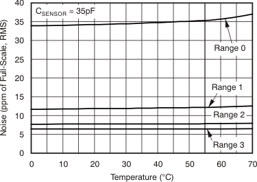
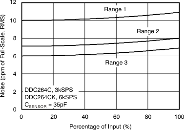
| Noise, low-level input(1) | Range = 3, CSENSOR(2) = 35 pF | 6.3 | ppm of FSR(3), rms | ||||
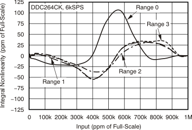
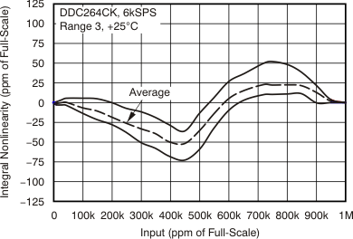
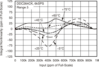
| Integral linearity error(4) | ±0.025% Reading ±1-ppm FSR | ±0.05% Reading ±1.5-ppm FSR |
|||||
| Resolution | No missing codes, format = 1 | 20 | Bits | ||||
| No missing codes, format = 0 | 16 | ||||||
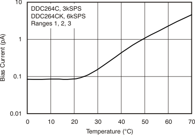
| Input bias current | TA = 25°C to 45°C | ±0.5 | ±5 | pA | |||
| Range error match(5) | 0.1% | 0.5% | FSR | ||||
| Range sensitivity to VREF | VREF = 4.096 ±0.1 V | 1:1 | |||||
| Offset error | ±500 | ±1000 | ppm of FSR | ||||
| Offset error match(5) | ±150 | ppm of FSR | |||||
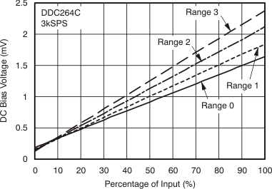
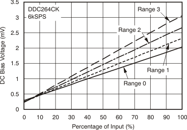
| DC bias voltage(6) | Low-level input (< 1% FSR) | ±0.1 | ±1 | mV | |||
| Power-supply rejection ratio | At DC | 100 | ±300 | ppm of FSR/V | |||
| PERFORMANCE OVER TEMPERATURE | |||||||
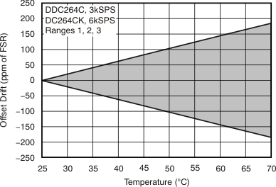
| Offset drift | ±0.5 | 5(7) | ppm of FSR/°C | ||||
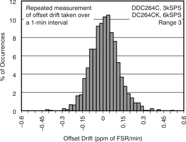
| Offset drift stability | ±0.2 | 2(7) | ppm of FSR/minute | ||||
| DC bias voltage drift(6) | ±3 | μV/°C | |||||
| Input bias current drift | TA = 25°C to 45°C | 0.01 | 1(7) | pA/°C | |||
| Range drift(8) | 25 | 50 | ppm/°C | ||||
| Range drift match(5) | ±5 | ppm/°C | |||||
| REFERENCE | |||||||
| Input current(9) | Average value with tINT = 333 µs | 825 | μA | ||||
| Average value with tINT = 166 µs (DDC264CK) | 1650 | μA | |||||
| DIGITAL INPUT AND OUTPUT | |||||||
| VIH | 0.8 × DVDD | DVDD + 0.1 | V | ||||
| VIL | –0.1 | 0.2 × DVDD | V | ||||
| VOH | IOH = –500 µA | DVDD – 0.4 | V | ||||
| VOL | IOL = 500 µA | 0.4 | V | ||||
| IIN | Input current | 0 < VIN < DVDD | ±10 | µA | |||
| Data format(10) | Straight binary | ||||||
| POWER-SUPPLY REQUIREMENTS | |||||||
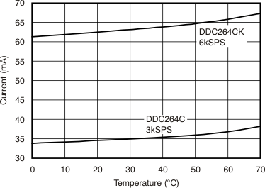
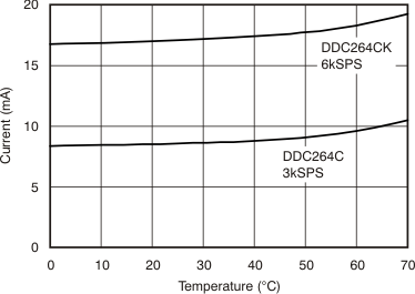
| Analog current | DDC264C | 34 | mA | ||||
| DDC264CK | 60 | ||||||
| Digital current | DDC264C | 7.5 | mA | ||||
| DDC264CK | 15 | ||||||
| Total power dissipation | DDC264C | 192 | 256 | mW | |||
| DDC264CK | 350 | ||||||
| Per channel power dissipation | DDC264C | 3 | 4 | mW/Channel | |||
| DDC264CK | 5.5 | ||||||
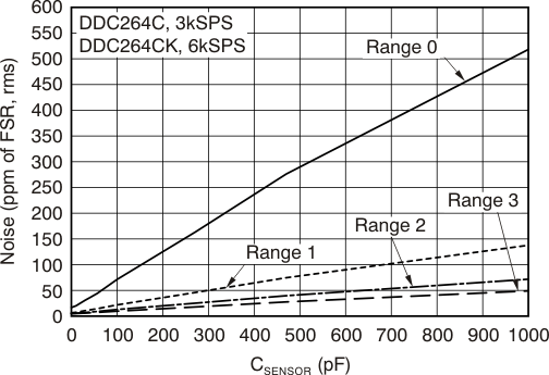
Table 1. NOISE vs CSENSOR(1)
| RANGE | CSENSOR | ||||||||
|---|---|---|---|---|---|---|---|---|---|
| 0 pF | 10 pF | 30 pF | 43 pF | 57 pF | 100 pF | 270 pF | 470 pF | 1000 pF | |
| ppm of FSR, rms | |||||||||
| Range 0: 12.5 pC | 16 | 20 | 30 | 37 | 44 | 71 | 160 | 270 | 510 |
| Range 1: 50 pC | 6.4 | 7.4 | 10 | 12 | 14 | 21 | 45 | 74 | 130 |
| Range 2: 100 pC | 5.1 | 5.5 | 7.1 | 8 | 9.1 | 12 | 25 | 39 | 71 |
| Range 3: 150 pC | 4.8 | 5 | 6 | 6.5 | 7.2 | 9.6 | 17 | 27 | 49 |
| fC, rms | |||||||||
| Range 0: 12.5 pC | 0.2 | 0.25 | 0.38 | 0.46 | 0.55 | 0.89 | 2 | 3.38 | 6.38 |
| Range 1: 50 pC | 0.32 | 0.37 | 0.53 | 0.62 | 0.73 | 1.09 | 2.29 | 3.73 | 6.88 |
| Range 2: 100 pC | 0.51 | 0.55 | 0.71 | 0.8 | 0.91 | 1.28 | 2.5 | 3.97 | 7.16 |
| Range 3: 150 pC | 0.72 | 0.75 | 0.9 | 0.98 | 1.08 | 1.45 | 2.67 | 4.14 | 7.36 |
| Electrons, rms | |||||||||
| Range 0: 12.5 pC | 1250 | 1560 | 2340 | 2890 | 3430 | 5540 | 12480 | 21070 | 39790 |
| Range 1: 50 pC | 2010 | 2310 | 3340 | 3910 | 4570 | 6800 | 14200 | 23300 | 42900 |
| Range 2: 100 pC | 3220 | 3440 | 4450 | 5000 | 5680 | 7990 | 15600 | 24800 | 44700 |
| Range 3: 150 pC | 4530 | 4730 | 5610 | 6120 | 6770 | 9050 | 16700 | 25800 | 45900 |
7.6 Typical Characteristics
at TA = 25°C (unless otherwise noted)