SBAS368D May 2006 – December 2016 DDC264
PRODUCTION DATA.
- 1 Features
- 2 Applications
- 3 Description
- 4 Revision History
- 5 Device Comparison Table
- 6 Pin Configuration and Functions
- 7 Specifications
-
8 Detailed Description
- 8.1 Overview
- 8.2 Functional Block Diagram
- 8.3
Feature Description
- 8.3.1 Dual Switched Integrator: Basic Integration Cycle
- 8.3.2 Integration Capacitors
- 8.3.3 Voltage Reference
- 8.3.4 Serial Data Output and Control Interface
- 8.4 Device Functional Modes
- 8.5 Programming
- 8.6 Register Maps
- 9 Application and Implementation
- 10Power Supply Recommendations
- 11Layout
- 12Device and Documentation Support
- 13Mechanical, Packaging, and Orderable Information
Package Options
Mechanical Data (Package|Pins)
- ZAW|100
Thermal pad, mechanical data (Package|Pins)
Orderable Information
8 Detailed Description
8.1 Overview
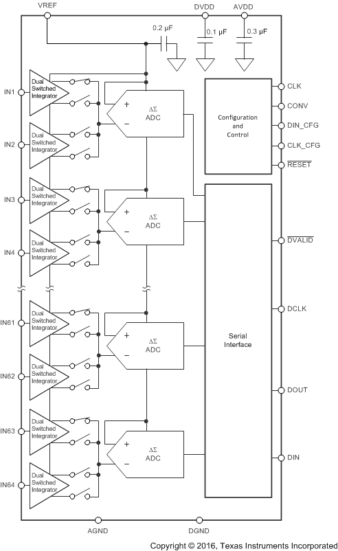
The DDC264 contains 64 identical input channels (see Functional Block Diagram) that perform the function of current-to-voltage integration followed by a multiplexed A/D conversion. Each input has two integrators (see Figure 18) so that the current-to-voltage integration can be continuous in time. The DDC264 continuously integrates the input signal by switching integrations between side A and side B.
For example, while side A integrates the input signal, the side B outputs are digitized by the onboard ADC. This integration and A/D conversion process is controlled by the convert pin, CONV. The results from side A and side B of each signal input are stored in a serial output shift register. The DVALID output goes low when the shift register data are ready to be retrieved.
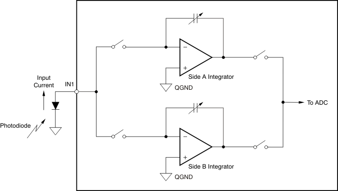 Figure 18. Dual Switched Integrator Architecture
Figure 19 shows a few integration cycles beginning after the device has been powered up, reset, and the Configuration Register has been programmed. The top signal is CONV and is supplied by the user. The integration status trace indicates which side is integrating. The output digital interface of the DDC264 sends the digital results through a synchronous serial interface that consists of a data clock (DCLK), a valid data pin (DVALID), a serial data output pin (DOUT), and a serial data input pin (DIN). As described above, DVALID goes active low when data are ready to be retrieved from the DDC264. It stays low until DCLK is taken high and then back low by the user. The text below the DVALID pulse indicates the side of the data available to be read. The arrow is used to match the data to the corresponding integration. Table 2 shows the timing specifications for Figure 19.
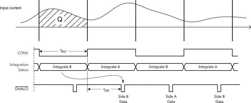 Figure 19. Integration Sequence Timing
Table 2. Timing Requirements for Integration Sequence Timing
| MIN | TYP | MAX | UNIT | |||
|---|---|---|---|---|---|---|
| tINT | Integration time | DDC264C(1) | 320 | 1,000,000 | µs | |
| DDC264CK(2) | 160 | |||||
| tDR | Time until data ready | DDC264C(1) | 276.4 ±0.4 | µs | ||
| DDC264CK(2) | 138.2 ±0.2 | |||||
Finally, a second set of digital signals (DIN_CFG and CLK_CFG pins, see Configuration Register — Read and Write Operations) is used to configure the DDC264 by addressing a dedicated register.
8.2 Functional Block Diagram
8.3 Feature Description
8.3.1 Dual Switched Integrator: Basic Integration Cycle
The topology of the front end of the DDC264 is an analog integrator as shown in Figure 20. In this diagram, only input IN1 is shown. The input stage consists of an operational amplifier, a selectable feedback capacitor network (CF), and several switches that implement the integration cycle. The timing relationships of all of the switches shown in Figure 20 are illustrated in Figure 21. Figure 21 conceptualizes the operation of the integrator input stage of the DDC264 and must not be used as an exact timing tool for design.
See Figure 22 for the block diagrams of the reset, integrate, wait, and convert states of the integrator section of the DDC264. This internal switching network is controlled externally with the convert pin (CONV) and the system clock (CLK). For the best noise performance, CONV must be synchronized with the falling edge of CLK. TI recommends toggling CONV within ±10 ns of the falling edge of CLK.
The noninverting inputs of the integrators are connected to the QGND pin. Consequently, the DDC264 analog ground, QGND, must be as clean as possible. In Figure 20, the feedback capacitors (CF) are shown in parallel between the inverting input and output of the operational amplifier. At the beginning of a conversion, the switches SA/D, SINTA, SINTB, SREF1, SREF2, and SRESET are set (see Figure 21).
At the completion of an A/D conversion, the charge on the integration capacitor (CF) is reset with SREF1 and SRESET (see Figure 21 and Figure 22a). This process is done during reset. In this manner, the selected capacitor is charged to the reference voltage, VREF. Once the integration capacitor is charged, SREF1 and SRESET are switched so that VREF is no longer connected to the amplifier circuit while it waits to begin integrating (see Figure 22b). With the rising edge of CONV, SINTA closes, which begins the integration of side A. This process puts the integrator stage into its integrate mode (see Figure 22c).
Charge from the input signal is collected on the integration capacitor, causing the voltage output of the amplifier to decrease. The falling edge of CONV stops the integration by switching the input signal from side A to side B (SINTA and SINTB). Prior to the falling edge of CONV, the signal on side B was converted by the A/D converter and reset during the time that side A was integrating. With the falling edge of CONV, side B starts integrating the input signal. At this point, the output voltage of the side A operational amplifier is presented to the input of the A/D converter (see Figure 22d).
A special elecrostatic discharge (ESD) structure protects the inputs but does not increase current leakage on the input pins.
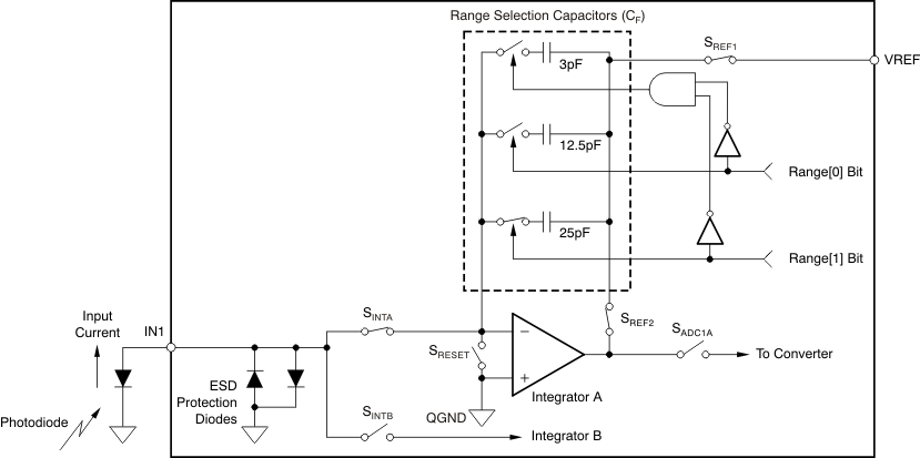 Figure 20. Basic Integration Configuration
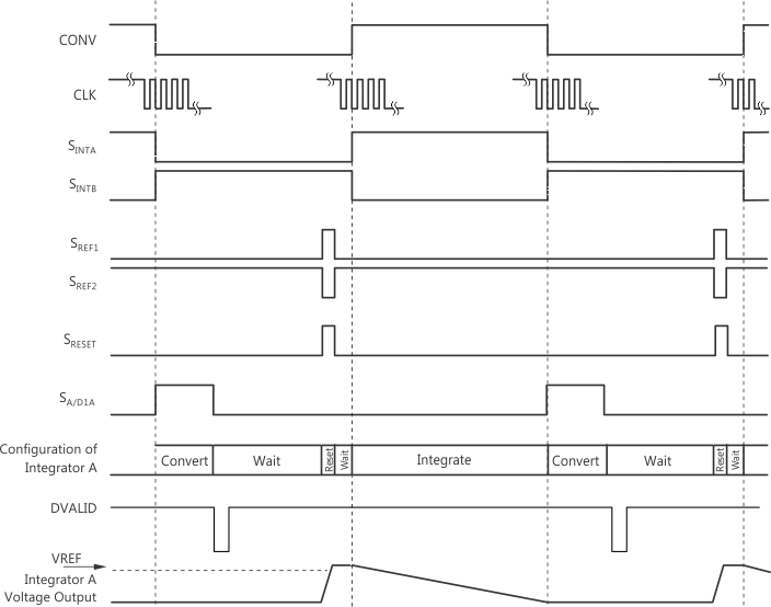 Figure 21. Integration Timing (see Figure 20)
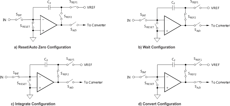 Figure 22. Four Configurations of the Front-End Integrators
8.3.2 Integration Capacitors
There are four different capacitor configurations available on-chip for both sides of every channel in the DDC264. These internal capacitors are trimmed in production to achieve the specified performance for range error of the DDC264. The range control bits (Range[1:0]) set the capacitor value for all integrators. Consequently, all inputs and both sides of each input always have the same full-scale range. Table 3 shows the capacitor value selected for each range selection.
Table 3. Range Selection
| RANGE | RANGE CONTROL BITS | CF | INPUT RANGE | |
|---|---|---|---|---|
| Range[1] | Range[0] | |||
| 0 | 0 | 0 | 3 pF | –0.04 to 12.5 pC |
| 1 | 0 | 1 | 12.5 pF | –0.2 to 50 pC |
| 2 | 1 | 0 | 25 pF | –0.4 to 100 pC |
| 3 | 1 | 1 | 37.5 pF | –0.6 to 150 pC |
8.3.3 Voltage Reference
The external voltage reference is used to reset the integration capacitors before an integration cycle begins. It is also used by the A/D converter while the converter is measuring the voltage stored on the integrators after an integration cycle ends. During this sampling, the external reference must supply the charge required by the A/D converter. For an integration time of 333 µs, this charge translates to an average VREF current of approximately 825 µA. The amount of charge required by the A/D converter is independent of the integration time; therefore, increasing the integration time lowers the average current. For example, an integration time of 800 µs lowers the average VREF current to 340 µA.
8.3.4 Serial Data Output and Control Interface
8.3.4.1 System and Data Clocks (CLK and DCLK)
The device internal clock is derived directly or after a divide by 4 from the CLK input (see Bit[13] in the configuration register). TI recommends driving the CLK pin with a free-running clock source (that is, do not start and stop CLK between conversions). Make sure the clock signals are clean—avoid overshoot or ringing.
As explained in Overview, DCLK is used to read out the data (more details in the following sections). For best performance, generate CLK and DCLK clocks from the same clock source. Disable DCLK by taking it low after the data have been shifted out and while CONV is transitioning.
When using multiple DDC264 devices, pay close attention to the DCLK distribution on the printed-circuit board (PCB). In particular, make sure to minimize skew in the DCLK signal because this can lead to timing violations in the serial interface specifications. See Cascading Multiple Converters for more details.
8.3.4.2 CONV: Setting the Integration Time
As explained in Overview, one integration cycle happens between two consecutive CONV signal edges. For the best noise performance, CONV must be synchronized with the falling edge of CLK. TI recommends toggling CONV within ±10 ns of the falling edge of CLK.
The minimum tINT for the DDC264 scales directly with the internal clock frequency. With an internal clock frequency of 10 MHz, the minimum time is 160 μs, which is achieved with the right register settings (see Configuration Register — Read and Write Operations for more details). If the minimum integration time is violated, the DDC264 stops continuously integrating the input signal. To return to normal operation (that is, continuous integration) after a violation of the minimum tINT specification, perform three integrations that each last for a minimum of 5000 internal clock periods. In other words, integrate three times with each integration lasting for at least 1 ms when using an internal clock frequency of 5 MHz. During this time, ignore the DVALID pin. Once the three integrations complete, normal continuous operation resumes, and data can be retrieved.
8.3.4.3 Data Valid (DVALID)
The DVALID signal indicates that data are ready to be read. Data retrieval may begin after DVALID goes low. This signal is generated using an internal clock divided down from the system clock, CLK. The phase relationship between this internal clock and CLK is set when power is first applied and is random. Because the user must synchronize CONV with CLK, the DVALID signal has a random phase relationship with CONV. This uncertainty is ±1/fCLK. Polling DVALID eliminates any concern about this relationship. If the data readback is timed from CONV, make sure to wait for the required amount of time. The data stored internally is lost if not read before the next DVALID.
8.3.4.4 Data Format
The serial output data are provided in an offset binary code as shown in Table 4. The format bit in the configuration register selects how many bits are used in the output word. When format = 1, 20 bits are used. When format = 0, the lower four bits are truncated so that only 16 bits are used. Note that the LSB size is 16 times bigger when format = 0. An offset is included in the output to allow slightly negative inputs (for example, from board leakages) from clipping the reading. This offset is approximately 0.4% of the positive full-scale.
Table 4. Ideal Output Code vs Input Signal(1)
| INPUT SIGNAL | IDEAL OUTPUT CODE FORMAT = 1 | IDEAL OUTPUT CODE FORMAT = 0 |
|---|---|---|
| ≥ 100% FS | 1111 1111 1111 1111 1111 | 1111 1111 1111 1111 |
| 0.001531% FS | 0000 0001 0000 0001 0000 | 0000 0001 0000 0001 |
| 0.001436% FS | 0000 0001 0000 0000 1111 | 0000 0001 0000 0000 |
| 0.000191% FS | 0000 0001 0000 0000 0010 | 0000 0001 0000 0000 |
| 0.000096% FS | 0000 0001 0000 0000 0001 | 0000 0001 0000 0000 |
| 0% FS | 0000 0001 0000 0000 0000 | 0000 0001 0000 0000 |
| –0.3955% FS | 0000 0000 0000 0000 0000 | 0000 0000 0000 0000 |
8.3.4.5 Data Retrieval
The data from the last conversion are available for retrieval on the falling edge of DVALID (see Figure 23 and Table 5). Data are shifted out on the falling edge of the data clock, DCLK.
Make sure not to retrieve data around changes in CONV because this change can introduce noise. Stop activity on DCLK at least 2 µs before or after a CONV transition.
Setting the format bit = 0 (16-bit output word) reduces the time required to retrieve data by 20% because there are fewer bits to shift out. This technique can be useful in multichannel systems requiring only 16 bits of resolution.
 Figure 23. Digital Interface Timing Diagram for Data Retrieval From a Single DDC264
Table 5. Timing for DDC264 Data Retrieval
| MIN | TYP | MAX | UNIT | ||
|---|---|---|---|---|---|
| tPDCDV | Propagation delay from falling edge of CLK to DVALID Low | 10 | ns | ||
| tPDDCDV | Propagation delay from falling edge of DCLK to DVALID High | 5 | ns | ||
| tHDDODV | Hold time that DOUT is valid before the falling edge of DVALID | 400 | ns | ||
| tHDDODC | Hold time that DOUT is valid after falling edge of DCLK | 4 | ns | ||
| tPDDCDO | Propagation delay from falling edge of DCLK to valid DOUT | 25 | ns | ||
8.3.4.5.1 Cascading Multiple Converters
Multiple DDC264 devices can be connected in a serial configuration; see Figure 24.
DOUT can be used with DIN to daisy-chain multiple DDC264 devices together to minimize wiring. In this mode of operation, the serial data output is shifted through multiple DDC264s; see Figure 24.
Figure 25 shows the timing diagram when the DIN input is used to daisy-chain several devices. Table 6 gives the timing specification for data retrieval using DIN.
 Figure 24. Daisy-Chained DDC264s
Table 6. Timing for DDC264 Data Retrieval Using DIN
| MIN | TYP | MAX | UNIT | ||
|---|---|---|---|---|---|
| tSTDIDC | Setup time from DIN to falling edge of DCLK | 10 | ns | ||
| tHDDIDC | Hold time for DIN after falling edge of DCLK | 10 | ns | ||
8.3.4.5.2 Retrieval Before CONV Toggles
In this method, data retrieval begins soon after DVALID goes low and finishes before CONV toggles, as shown in Figure 26. For best performance, data retrieval must stop tSDCV before CONV toggles. This method is most appropriate for longer integration times and yields the best performance results as the output interface toggling noise does not interfere with the ADC conversion operation. The maximum time available for readback is
tINT – tCMDR – tSDCV. The maximum number of DDC264s that can be daisy-chained together (format = 1) is calculated by Equation 1.

For example, if tINT = 1000 µs and DCLK = 20 MHz, the maximum number of DDC264s with format = 1 is shown in Equation 2.

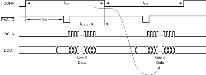 Figure 26. Readback Before CONV Toggles
Table 7. Timing for Readback
| MIN | TYP | MAX | UNIT | ||
|---|---|---|---|---|---|
| tSDCV | Data retrieval shutdown before or after edge of CONV | 2 | µs | ||
8.3.4.5.3 Retrieval After CONV Toggles
For shorter integration times, more time is available if data retrieval begins after CONV toggles and ends before the new data are ready. Data retrieval must wait tSDCV after CONV toggles before beginning. See Figure 27 for an example of this timing sequence. The maximum time available for retrieval is tDR – (tSDCV + tHDDODV), regardless of tINT. The maximum number of DDC264s that can be daisy-chained together with format = 1 is calculated by Equation 3.

For DCLK = 20 MHz, the maximum number of DDC264s is four (or five for format = 0).
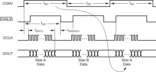 Figure 27. Readback After CONV Toggles
8.3.4.5.4 Retrieval Before and After CONV Toggles
For the absolute maximum time for data retrieval, data can be retrieved before and after CONV toggles. Nearly all of tINT is available for data retrieval. Figure 28 illustrates how this process is done by combining the two previous methods. Pause the retrieval during CONV toggling to prevent digital noise, as discussed previously, and finish before the next data are ready. The maximum number of DDC264s that can be daisy-chained together with format = 1 is calculated by Equation 4.

For tINT = 400 µs and DCLK = 20 MHz, the maximum number of DDC264s is six (or seven for format = 0).
 Figure 28. Readback Before and After CONV Toggles
8.4 Device Functional Modes
There are no functional modes for this device.
8.5 Programming
8.5.1 Reset (RESET)
The DDC264 is reset asynchronously by taking the RESET input low, as shown in Figure 29. Make sure the release pulse is a minimum of tRST wide. It is very important that RESET is glitch-free to avoid unintentional resets. The Configuration Register must be programmed immediately afterwards. After programming the DDC264, wait at least four conversions before using the data.
 Figure 29. Reset Timing
8.5.2 Configuration Register — Read and Write Operations
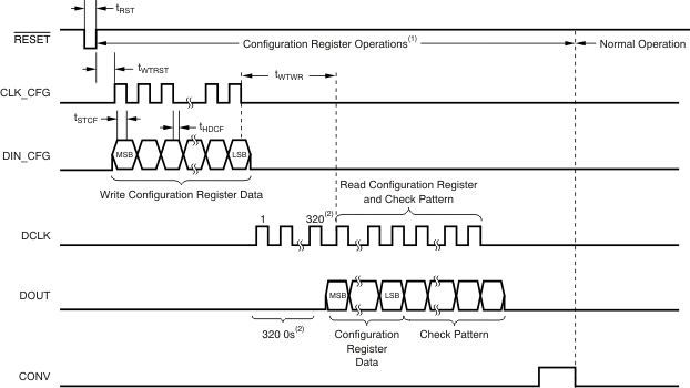
The Configuration Register must be programmed after power-up or a device reset. The DIN_CFG, CLK_CFG, and RESET pins are used to write to this register. When beginning a write operation, hold CONV low and strobe RESET; see Figure 30. Then begin shifting in the configuration data on DIN_CFG. Data are written to the Configuration Register most significant bit first. The data are internally latched on the falling edge of CLK_CFG. Partial writes to the Configuration Register are not allowed, that is, make sure to send all 16 bits when updating the register.
Optional readback of the Configuration Register is available immediately after the write sequence. During readback, 320 '0's, then the 16-bit configuration data followed by a 4-bit revision ID and the check pattern are shifted out on the DOUT pin on the rising edge of DCLK. The check pattern can be used to check or verify the DOUT functionality.
NOTE
With format = 1, the check pattern is 300 bits, with only the last 72 bits non-zero. This sequence of outputs is repeated twice for each DDC264 block and daisy-chaining is supported in configuration readback. Table 9 shows the check pattern configuration during readback. Table 8 shows the timing for the Configuration Register read and write operations. Strobe CONV to begin normal operation, that is, CONV must not toggle during the readback operation.
Table 8. Timing Requirements for the Configuration Register Read/Write
| MIN | TYP | MAX | UNIT | ||
|---|---|---|---|---|---|
| tWTRST | Wait Required from Reset High to First Rising Edge of CLK_CFG | 2 | µs | ||
| tWTWR | Wait Required from Last CLK_CFG of Write Operation to First DCLK of Read Operation |
2 | µs | ||
| tSTCF | Set-Up Time from DIN_CFG to Falling Edge of CLK_CFG | 10 | ns | ||
| tHDCF | Hold Time for DIN_CFG After Falling Edge of CLK_CFG | 10 | ns | ||
| tRST | Pulse Width for RESET Active | 1 | µs | ||
Table 9. Check Pattern During Readback
| FORMAT BIT | CHECK PATTERN (Hex) |
TOTAL READBACK BITS |
|---|---|---|
| 0 | 180 0s, 30F066012480F6h | 1024 |
| 1 | 228 0s, 30F066012480F69055h | 1280 |
8.6 Register Maps
Table 1. Configuration Register Bit Assignments
| BIT 15 | BIT 14 | BIT 13 | BIT 12 | BIT 11 | BIT 10 | BIT 9 | BIT 8 |
| 0 | 0 | Clkdiv | 0 | 0 | Range[1] | Range[0] | Format |
| BIT 7 | BIT 6 | BIT 5 | BIT 4 | BIT 3 | BIT 2 | BIT 1 | BIT 0 |
| Version | 0 | 0 | Reserved | 0 | 0 | 0 | Test |
| Bits 15:14 | These bits must always be set to 0. | |
| Bit 13 | Clkdiv | |
| The Clkdiv input enables an internal divider on the system clock as shown in Table 10. When Clkdiv = 1, the system clock is divided by 4. This configuration allows a system clock that is faster by a factor of four, which in turn provides a finer quantization of the integration time, because the CONV signal must be synchronized with the system clock for the best performance. | ||
| 0 = Internal clock divider set to 1 1 = Internal clock divider set to 4 |
||
Table 10. Clkdiv Operation
| Clkdiv BIT | CLK DIVIDER VALUE | CLK FREQUENCY | INTERNAL CLOCK FREQUENCY |
|---|---|---|---|
| 0 | 1 | 5 MHz | 5 MHz |
| 1 | 4 | 20 MHz | 5 MHz |
| Bits 12:11 | These bits must always be set to 0. | ||||
| Bits 10:9 | Range[1:0] | ||||
| These bits set the full-scale range. | |||||
| 00 = Range 0 01 = Range 1 |
= 12.5 pC = 50 pC |
10 = Range 2 11 = Range 3 |
= 100 pC = 150 pC |
||
| Bit 8 | Format | ||||
| Format selects how many bits are used in the data output word. | |||||
| 0 = 16-bit output 1 = 20-bit output |
|||||
| Bit 7 | Version | ||||
| This bit must be set to match the device being used. Must be set to 0 for DDC264C. Must be set to 1 for DDC264CK. |
|||||
| Bits 6:5 | These bits must always be set to 0. | ||||
| Bit 4 | Reserved | ||||
| This bit is reserved and must be set to 0. | |||||
| Bits 3:1 | These bits must always be set to 0. | ||||
| Bit 0 | Test | ||||
| When Test Mode is used, the inputs (IN1 through IN64) are disconnected from the DDC264 integrators to enable the user to measure a zero input signal regardless of the current supplied to the inputs. | |||||
| 0 = TEST mode off 1 = TEST mode on |
|||||
