SBASB20 September 2024 DDS39RF10 , DDS39RFS10
PRODUCTION DATA
- 1
- 1 Features
- 2 Applications
- 3 Description
- 4 Device Comparison
- 5 Pin Configuration and Functions
-
6 Specifications
- 6.1 Absolute Maximum Ratings
- 6.2 ESD Ratings
- 6.3 Recommended Operating Conditions
- 6.4 Thermal Information
- 6.5 Electrical Characteristics - DC Specifications
- 6.6 Electrical Characteristics - AC Specifications
- 6.7 Electrical Characteristics - Power Consumption
- 6.8 Timing Requirements
- 6.9 Switching Characteristics
- 6.10 SPI and FRI Timing Diagrams
- 6.11 Typical Characteristics: Single Tone Spectra
- 6.12 Typical Characteristics: Dual Tone Spectra
- 6.13 Typical Characteristics: Power Dissipation and Supply Currents
-
7 Detailed Description
- 7.1 Overview
- 7.2 Functional Block Diagrams
- 7.3
Feature Description
- 7.3.1 DAC Output Modes
- 7.3.2 DAC Core
- 7.3.3 DEM and Dither
- 7.3.4 Offset Adjustment
- 7.3.5 Clocking Subsystem
- 7.3.6 Digital Signal Processing Blocks
- 7.3.7
JESD204C Interface
- 7.3.7.1 Deviation from JESD204C Standard
- 7.3.7.2 Transport Layer
- 7.3.7.3 Scrambler and Descrambler
- 7.3.7.4 Link Layer
- 7.3.7.5 Physical Layer
- 7.3.7.6 Serdes PLL Control
- 7.3.7.7 Serdes Crossbar
- 7.3.7.8 Multi-Device Synchronization and Deterministic Latency
- 7.3.7.9 Operation in Subclass 0 Systems
- 7.3.7.10 Link Reset
- 7.3.8 Alarm Generation
- 7.4 Device Functional Modes
- 7.5 Programming
- 8 Application and Implementation
- 9 Device and Documentation Support
- 10Revision History
- 11Mechanical, Packaging, and Orderable Information
Package Options
Mechanical Data (Package|Pins)
Thermal pad, mechanical data (Package|Pins)
Orderable Information
7.3.7 JESD204C Interface
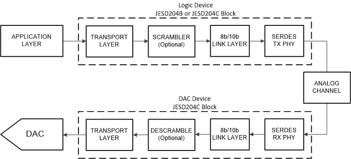
The devices uses a JESD204C high-speed serial interface to transfer data from the logic device to the receiving DAC. The device serial lanes are capable of operating with both 8b/10b encoding and 64b/66b encoding. The JESD204C formats using 8b/10b encoding are backwards compatible with existing JESD204B receivers. A maximum of 2 lanes can be used to lower lane rates for interfacing with speed limited logic devices. There are a few differences between 8b/10b and 64b/66b encoding, which is highlighted throughout this section. Figure 7-50 shows a simplified block diagram of the 8b/10b encoded JESD204C interface and Figure 7-51 shows a simplified block diagram of the 64b/66b encoded JESD204C interface.
 Figure 7-50 Simplified JESD204C Interface Diagram with 8b/10b Encoding
 Figure 7-51 Simplified JESD204C Interface Diagram with 64b/66b Encoding
Not all optional features of JESD204C are supported by the device. The list of features that are supported and the features that are not supported is provided in Table 7-15
| LETTER IDENTIFIER | FEATURE | SUPPORTED BY DEVICE? |
|---|---|---|
| a | 8b/10b link layer | Yes |
| b | 64b/66b link layer | Yes |
| c | 64b/80b link layer | No |
| d | The command channel when using 64b/66b or 64b/80b link layer | No |
| e | Forward error correction (FEC) when using the 64b/66b or 64b/80b link layer | No |
| f | CRC3 when using the 64b/66b or 64b/80b link layer | No |
| g | A physical SYNC pin when using the 8b/10b link layer | Yes |
| h | Subclass 0 | Yes |
| i | Subclass 1 | Yes |
| j | Subclass 2 | No |
| k | Lane alignment within a single link | Yes |
| l | Subclass 1 with support for lane alignment on a multipoint link by means of the MULTIREF signal | No |
| m | SYNC interface timing compatible with JESD204A | Yes |
| n | SYNC interface timing compatible with JESD204B | Yes |
The various signals used in the JESD204C interface and the associated device pin names are summarized briefly in Table 7-16 for reference.
| SIGNAL NAME | DEVICE PIN NAMES | DESCRIPTION |
|---|---|---|
| Data | 6SRX±, 14SRX± | High-speed serialized data after 8b/10b or 64b/66b encoding that is received by the SerDes receivers. |
| SYNC | SYNC | Link initialization signal (handshake), toggles low to start code group synchronization (CGS) process. Not used for 64B/66B encoding modes. |
| Device clock | CLK+, CLK– | DAC sampling clock, also used for clocking digital logic and SerDes receivers. |
| SYSREF | SYSREF+, SYSREF– | System timing reference used to deterministically reset the internal local multiframe clock (LMFC) or local extended multiblock clock (LEMC) counters in each JESD204C device |