DLPS140B March   2019  – May 2022 DLP2000

PRODUCTION DATA  

  1. Features
  2. Applications
  3. Description
  4. Revision History
  5. Pin Configuration and Functions
  6. Specifications
    1. 6.1  Absolute Maximum Ratings
    2. 6.2  Storage Conditions
    3. 6.3  ESD Ratings
    4. 6.4  Recommended Operating Conditions
    5. 6.5  Thermal Information
    6. 6.6  Electrical Characteristics
    7. 6.7  Timing Requirements
    8. 6.8  System Mounting Interface Loads
    9. 6.9  Physical Characteristics of the Micromirror Array
    10. 6.10 Micromirror Array Optical Characteristics
    11. 6.11 Window Characteristics
    12. 6.12 Chipset Component Usage Specification
  7. Detailed Description
    1. 7.1 Overview
    2. 7.2 Functional Block Diagram
    3. 7.3 Feature Description
      1. 7.3.1 Power Interface
      2. 7.3.2 Control Serial Interface
      3. 7.3.3 High Speed Interface
      4. 7.3.4 Timing
    4. 7.4 Device Functional Modes
    5. 7.5 Window Characteristics and Optics
      1. 7.5.1 Optical Interface and System Image Quality
        1. 7.5.1.1 Numerical Aperture and Stray Light Control
        2. 7.5.1.2 Pupil Match
        3. 7.5.1.3 Illumination Overfill
    6. 7.6 Micromirror Array Temperature Calculation
    7. 7.7 Micromirror Landed-On/Landed-Off Duty Cycle
      1. 7.7.1 Definition of Micromirror Landed-On/Landed-Off Duty Cycle
      2. 7.7.2 Landed Duty Cycle and Useful Life of the DMD
      3. 7.7.3 Landed Duty Cycle and Operational DMD Temperature
      4. 7.7.4 Estimating the Long-Term Average Landed Duty Cycle of a Product or Application
  8. Application and Implementation
    1. 8.1 Application Information
    2. 8.2 Typical Application
      1. 8.2.1 Design Requirements
      2. 8.2.2 Detailed Design Procedure
      3. 8.2.3 Application Curve
  9. Power Supply Recommendations
    1. 9.1 Power Supply Power-Up Procedure
    2. 9.2 Power Supply Power-Down Procedure
  10. 10Layout
    1. 10.1 Layout Guidelines
    2. 10.2 Layout Example
  11. 11Device and Documentation Support
    1. 11.1 Third-Party Products Disclaimer
    2. 11.2 Device Support
      1. 11.2.1 Device Nomenclature
      2. 11.2.2 Device Markings
    3. 11.3 Related Links
    4. 11.4 Receiving Notification of Documentation Updates
    5. 11.5 Support Resources
    6. 11.6 Trademarks
    7. 11.7 Electrostatic Discharge Caution
    8. 11.8 Glossary
  12. 12Mechanical, Packaging, and Orderable Information

Package Options

Mechanical Data (Package|Pins)
Thermal pad, mechanical data (Package|Pins)
Orderable Information

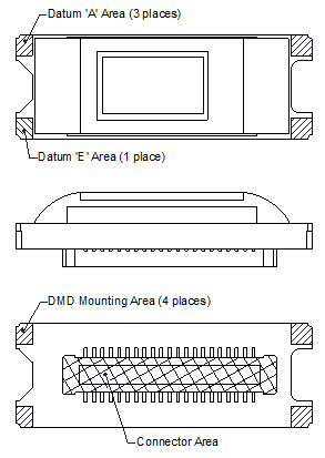
System Mounting Interface Loads

over operating free-air temperature range (unless otherwise noted)
PARAMETER MIN NOM MAX UNIT
Maximum system mounting interface load to be applied to the: Connector area (See Figure 6-7.) 45 N
DMD mounting area uniformly distributed over 4 areas (See Figure 6-7.) 100 N
GUID-8B17FDA5-9FD3-419A-9A63-535A2EAFBB85-low.gifFigure 6-7 System Interface Loads