DLPS214B July   2021  – May 2022 DLP300S

PRODUCTION DATA  

  1. Features
  2. Applications
  3. Description
  4. Revision History
  5. Pin Configuration and Functions
  6. Specifications
    1. 6.1  Absolute Maximum Ratings
    2. 6.2  Storage Conditions
    3. 6.3  ESD Ratings
    4. 6.4  Recommended Operating Conditions
    5. 6.5  Thermal Information
    6. 6.6  Electrical Characteristics
    7. 6.7  Timing Requirements
    8. 6.8  Switching Characteristics
    9. 6.9  System Mounting Interface Loads
    10. 6.10 Micromirror Array Physical Characteristics
    11. 6.11 Micromirror Array Optical Characteristics
    12. 6.12 Window Characteristics
    13. 6.13 Chipset Component Usage Specification
    14. 6.14 Software Requirements
  7. Detailed Description
    1. 7.1 Overview
    2. 7.2 Functional Block Diagram
    3. 7.3 Feature Description
      1. 7.3.1 Power Interface
      2. 7.3.2 Low-Speed Interface
      3. 7.3.3 High-Speed Interface
      4. 7.3.4 Timing
    4. 7.4 Device Functional Modes
    5. 7.5 Optical Interface and System Image Quality Considerations
      1. 7.5.1 Optical Interface and System Image Quality
        1. 7.5.1.1 Numerical Aperture and Stray Light Control
        2. 7.5.1.2 Pupil Match
        3. 7.5.1.3 Illumination Overfill
    6. 7.6 Micromirror Array Temperature Calculation
    7. 7.7 Micromirror Landed-On/Landed-Off Duty Cycle
      1. 7.7.1 Definition of Micromirror Landed-On and Landed-Off Duty Cycle
      2. 7.7.2 Landed Duty Cycle and Useful Life of the DMD
      3. 7.7.3 Landed Duty Cycle and Operational DMD Temperature
      4. 7.7.4 Estimating the Long-Term Average Landed Duty Cycle of a Product or Application
  8. Application and Implementation
    1. 8.1 Application Information
    2. 8.2 Typical Application
      1. 8.2.1 Design Requirements
      2. 8.2.2 Detailed Design Procedure
      3. 8.2.3 Application Curve
  9. Power Supply Recommendations
    1. 9.1 DMD Power Supply Power-Up Procedure
    2. 9.2 DMD Power Supply Power-Down Procedure
    3. 9.3 Power Supply Sequencing Requirements
  10. 10Layout
    1. 10.1 Layout Guidelines
    2. 10.2 Layout Example
  11. 11Device and Documentation Support
    1. 11.1 Device Support
      1. 11.1.1 Third-Party Products Disclaimer
      2. 11.1.2 Device Nomenclature
      3. 11.1.3 Device Markings
    2. 11.2 Receiving Notification of Documentation Updates
    3. 11.3 Related Links
    4. 11.4 Support Resources
    5. 11.5 Trademarks
    6. 11.6 Electrostatic Discharge Caution
    7. 11.7 Glossary
  12. 12Mechanical, Packaging, and Orderable Information

Package Options

Mechanical Data (Package|Pins)
Thermal pad, mechanical data (Package|Pins)
Orderable Information

Typical Application

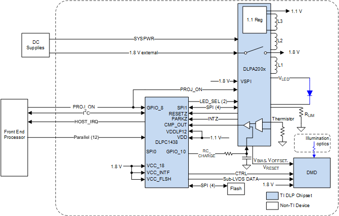
Figure 8-1 and Figure 8-2 show typical DLP 3D printer system block diagrams using the DLP300S DMD, DLPC1438 controller, and DLPA200x PMIC/LED driver.
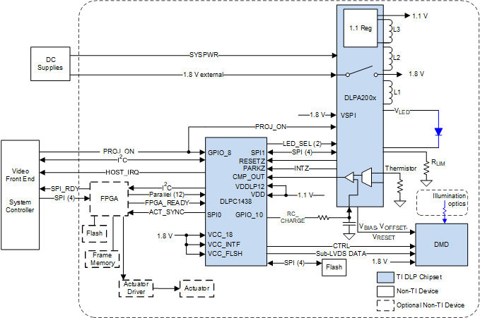
GUID-60D2BE12-A7EF-4948-8445-A45BFC929FB5-low.gifFigure 8-1 With FPGA
GUID-F445069A-63B5-4FAF-8F6D-87D82621B2CB-low.gifFigure 8-2 Without FPGA