DLPS081 February 2022 DLP3020-Q1
PRODUCTION DATA
- 1 Features
- 2 Applications
- 3 Description
- 4 Revision History
- 5 Pin Configuration and Functions
-
6 Specifications
- 6.1 Absolute Maximum Ratings
- 6.2 Storage Conditions
- 6.3 ESD Ratings
- 6.4 Recommended Operating Conditions
- 6.5 Thermal Information
- 6.6 Electrical Characteristics
- 6.7 Timing Requirements
- 6.8 Switching Characteristics
- 6.9 System Mounting Interface Loads
- 6.10 Physical Characteristics of the Micromirror Array
- 6.11 Micromirror Array Optical Characteristics
- 6.12 Window Characteristics
- 6.13 Chipset Component Usage Specification
- 7 Detailed Description
- 8 Application and Implementation
- 9 Power Supply Recommendations
- 10Layout
- 11Device and Documentation Support
- 12Mechanical, Packaging, and Orderable Information
Package Options
Mechanical Data (Package|Pins)
- FQR|54
Thermal pad, mechanical data (Package|Pins)
Orderable Information
6.7 Timing Requirements
Over Section 6.4 unless otherwise noted.
| MIN | NOM | MAX | UNIT | ||
|---|---|---|---|---|---|
| DMD MIRROR AND SRAM CONTROL LOGIC SIGNALS | |||||
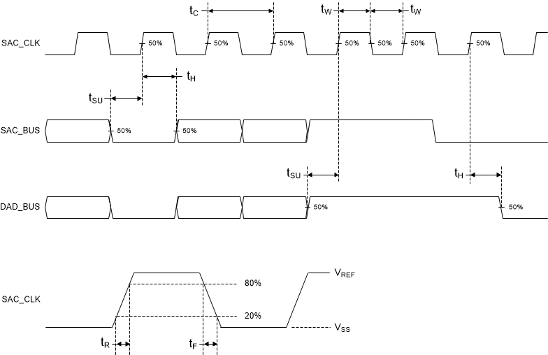
| tSU | Setup time SAC_BUS low before SAC_CLK↑ | 1.0 | ns | ||
| tH | Hold time SAC_BUS low after SAC_CLK↑ | 1.0 | ns | ||
| tSU | Setup time DAD_BUS high before SAC_CLK↑ | 1.0 | ns | ||
| tH | Hold time DAD_BUS after SAC_CLK↑ | 1.0 | ns | ||
| tC | Cycle time SAC_CLK | 12.5 | 16.67 | ns | |
| tW | Pulse width 50% to 50% reference points: SAC_CLK high or low | 5.0 | ns | ||
| tR | Rise time 20% to 80% reference points: SAC_CLK | 2.5 | ns | ||
| tF | Fall time 80% to 20% reference points: SAC_CLK | 2.5 | ns | ||
| DMD DATA PATH AND LOGIC CONTROL SIGNALS | |||||
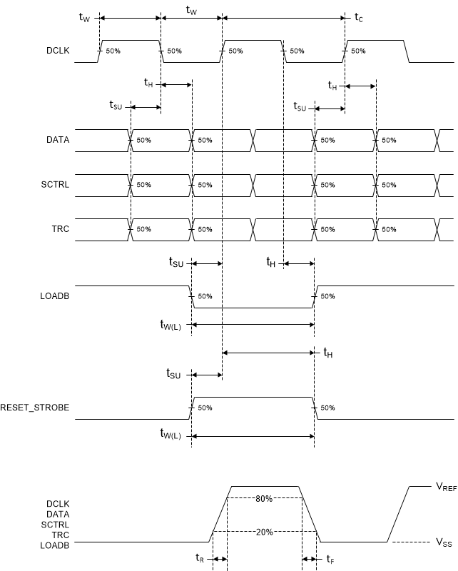
| tSU | Setup time DATA(14:0) before DCLK↑ or DCLK↓ | 1.0 | ns | ||
| tH | Hold time DATA(14:0) after DCLK↑ or DCLK↓ | 1.0 | ns | ||
| tSU | Setup time SCTRL before DCLK↑ or DCLK↓ | 1.0 | ns | ||
| tH | Hold time SCTRL after DCLK↑ or DCLK↓ | 1.0 | ns | ||
| tSU | Setup time TRC before DCLK↑ or DCLK↓ | 1.0 | ns | ||
| tH | Hold time TRC after DCLK↑ or DCLK↓ | 1.0 | ns | ||
| tSU | Setup time LOADB low before DCLK↑ | 1.0 | ns | ||
| tH | Hold time LOADB low after DCLK↓ | 1.0 | ns | ||
| tSU | Setup time RESET_STROBE high before DCLK↑ | 1.0 | ns | ||
| tH | Hold time RESET_STROBE after DCLK↑ | 3.5 | ns | ||
| tC | Cycle time DCLK | 12.5 | 16.67 | ns | |
| tW | Pulse width 50% to 50% reference points: DCLK high or low | 5.0 | ns | ||
| tW(L) | Pulse width 50% to 50% reference points: LOADB low | 7.0 | ns | ||
| tW(H) | Pulse width 50% to 50% reference points: RESET_STROBE high | 7.0 | ns | ||
| tR | Rise time 20% to 80% reference points: DCLK, DATA, SCTRL, TRC, LOADB | 2.5 | ns | ||
| tF | Fall time 80% to 20% reference points: DCLK, DATA, SCTRL, TRC, LOADB | 2.5 | ns | ||
| JTAG BOUNDARY SCAN CONTROL LOGIC SIGNALS | |||||
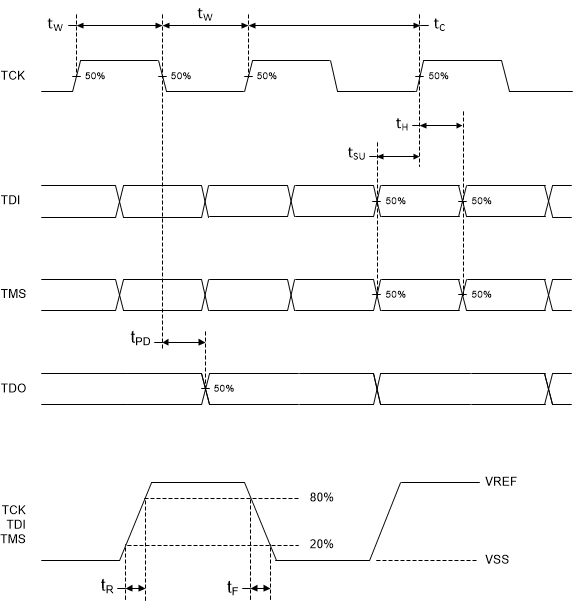
| fTCK | Clock frequency TCK | 10 | MHz | ||
| tC | Cycle time TCK | 100 | ns | ||
| tW | Pulse width 50% to 50% reference points: TCK high or low | 10 | ns | ||
| tSU | Setup time TDI valid before TCK↑ | 5 | ns | ||
| tH | Hold time TDI valid after TCK↑ | 25 | ns | ||
| tSU | Setup time TMS valid before TCK↑ | 5 | ns | ||
| tH | Hold time TMS valid after TCK↑ | 25 | ns | ||
| tR | Rise time 20% to 80% reference points: TCK, TDI, TMS | 2.5 | ns | ||
| tR | Fall time 80% to 20% reference points: TCK, TDI, TMS | 2.5 | ns | ||
 Figure 6-2 DMD Mirror and SRAM Control Logic Timing Requirements
 Figure 6-3 DMD Data Path and Control Logic Timing Requirements
 Figure 6-4 JTAG Boundary Scan Control Logic Timing Requirements