DLPS081 February 2022 DLP3020-Q1
PRODUCTION DATA
- 1 Features
- 2 Applications
- 3 Description
- 4 Revision History
- 5 Pin Configuration and Functions
-
6 Specifications
- 6.1 Absolute Maximum Ratings
- 6.2 Storage Conditions
- 6.3 ESD Ratings
- 6.4 Recommended Operating Conditions
- 6.5 Thermal Information
- 6.6 Electrical Characteristics
- 6.7 Timing Requirements
- 6.8 Switching Characteristics
- 6.9 System Mounting Interface Loads
- 6.10 Physical Characteristics of the Micromirror Array
- 6.11 Micromirror Array Optical Characteristics
- 6.12 Window Characteristics
- 6.13 Chipset Component Usage Specification
- 7 Detailed Description
- 8 Application and Implementation
- 9 Power Supply Recommendations
- 10Layout
- 11Device and Documentation Support
- 12Mechanical, Packaging, and Orderable Information
Package Options
Mechanical Data (Package|Pins)
- FQR|54
Thermal pad, mechanical data (Package|Pins)
Orderable Information
6.8 Switching Characteristics
Over operating free-air temperature range (unless otherwise noted).(1)
| PARAMETER | TEST CONDITIONS | MIN | TYP | MAX | UNIT | |
|---|---|---|---|---|---|---|
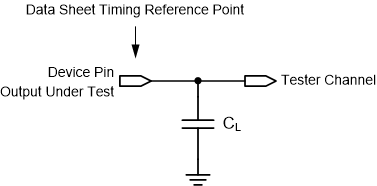
| tPD | Output propagation, clock to Q (see Figure 6-4) | CL = 11 pF, from (Input) falling edge of TCK to (Output) TDO, see Figure 6-4 | 3 | 25 | ns | |
(1) Device electrical characteristics are over Recommended Operating Characteristics
unless otherwise noted.
 Figure 6-5 Test Load Circuit for Output Propagation Measurement